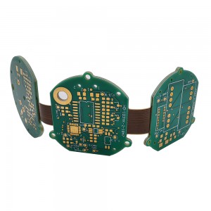
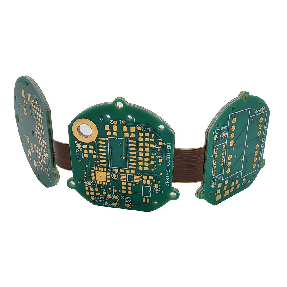
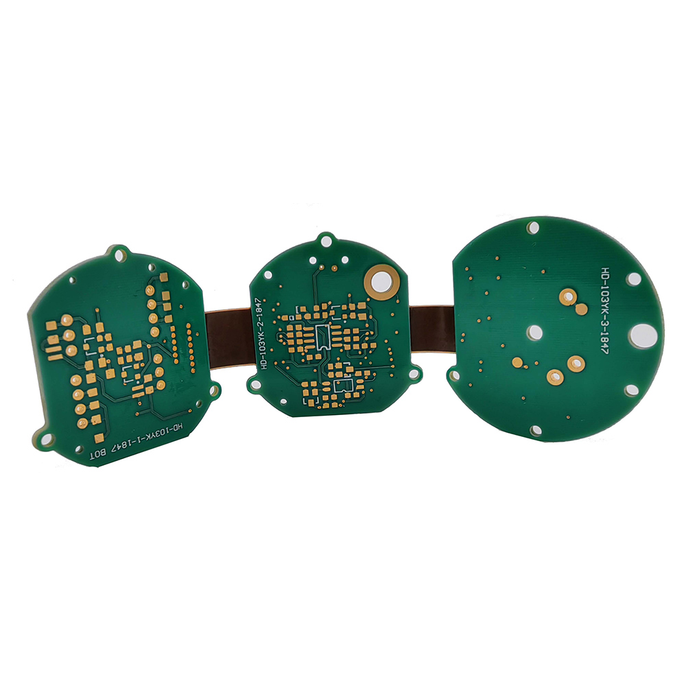
Customized Wearable 4 Layers Rigid-Flex PCB circuit board China FPC
Basic Info
| Model No. | PCB-A6 |
| Transport package | Vacuum Packing |
| Certification | UL,ISO9001&ISO14001,RoHS |
| Minimum Space/Line | 0.075mm/3mil |
| Impedance control | 100±10% |
| Production Capacity | 720, 000 M2/Year |
| Origin | Made in China |
| Application | Consumer electronics |
Product Description
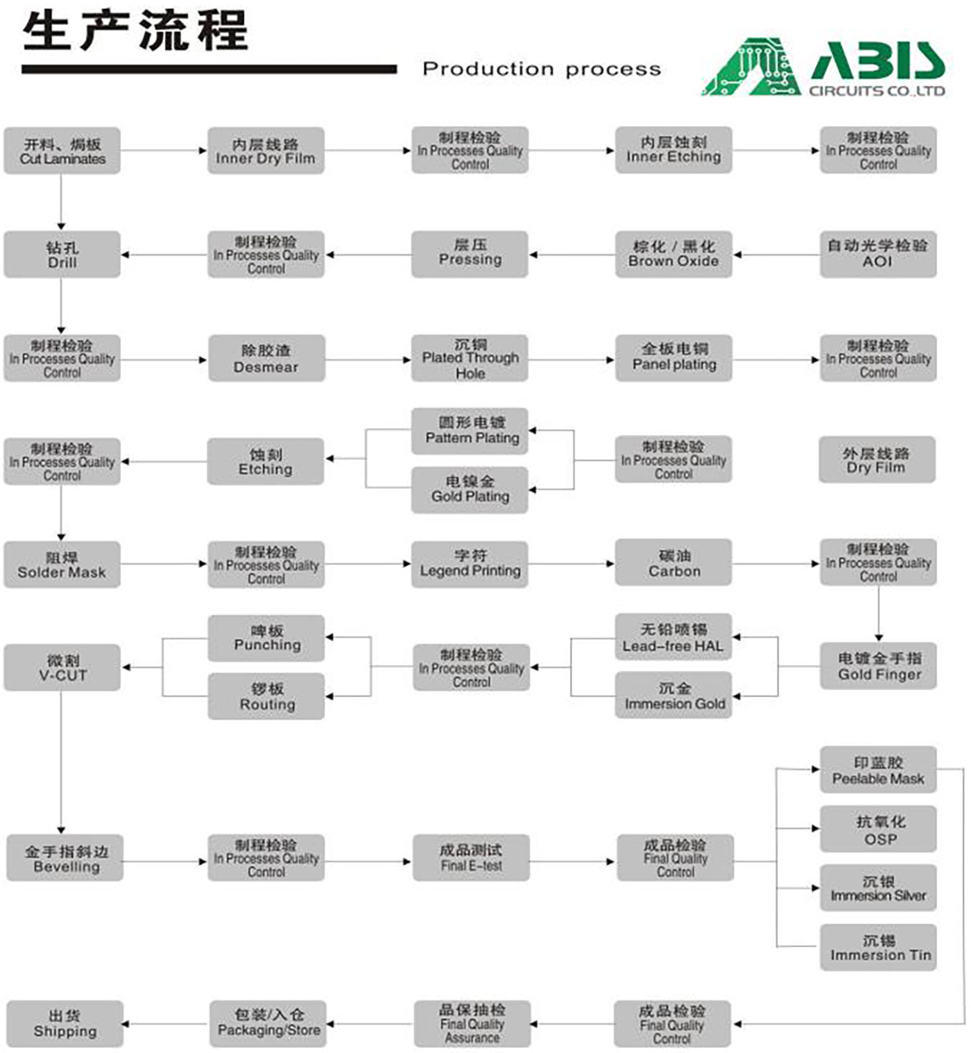
How ABIS Handling the Rigid-Flexible Circuit?
The capability to shape the final assembly of rigid and flexible PCBs to fit a product enclosure is the primary advantage of flexible circuits boards. Here are 2 tips to incorporate in your rigid-flex design project:
Increase trace reliability: The bending that flex circuits endure means that the copper is more likely to delaminate than on a rigid board. The addition of copper to the substrate is less than on an FR4 PCB as well.
Strengthen traces and vias with teardrops: If not controlled, bending the substrate can lead to delamination and product failure. Traces and vias can, however, be strengthened to prevent delamination, also produce better yield in manufacturing by giving more drilling tolerance.
Technical & Capability
|
Item |
Spec. |
|
Layers |
1~8 |
|
Board Thickness |
0.1mm-8.0mm |
|
Material |
Polymide, PET, PEN, FR4 |
|
Max Panel Size |
600mm×1200mm |
|
Min Hole Size |
0.1mm |
|
Min Line Width/Space |
3mil(0.075mm) |
|
Board Outline Tolerance |
士0.10mm |
|
Insulation Layer Thickness |
0.075mm--5.00mm |
|
Final Thickness |
0.0024''-0.16'' (0.06-2.4.00mm) |
|
Drilling Hole (Mechanical) |
17um--175um |
|
Finish Hole (Mechanical) |
0.10mm--6.30mm |
|
Diameter Tolerance (Mechanical) |
0.05mm |
|
Registration (Mechanical) |
0.075mm |
|
Aspect Ratio |
16:1 |
|
Solder Mask Type |
LPI |
|
SMT Mini. Solder Mask Width |
0.075mm |
|
Mini. Solder Mask Clearance |
0.05mm |
|
Plug Hole Diameter |
0.25mm--0.60mm |
|
Impedance Control Tolerance |
士10% |
|
Surface finish |
ENIG, Chem. Tin/Sn, Flash Gold |
|
Solder mask |
Green/Yellow/Black/White/Red/Blue |
|
Silkscreen |
Red/Yellow/Black/White |
|
Certificate |
UL, ISO 9001, ISO14001, IATF16949 |
|
Special Request |
Blind hole, Gold finger, BGA, Carbon ink, peekable mask, VIP process, Edge plating, Half holes |
|
Material Suppliers |
Shengyi, ITEQ, Taiyo, etc. |
|
Common Package |
Vacuum+Carton |
Flexible PCB Lead Time
|
Small Batch Volume ≤1 sq meter |
Working Days |
Mass Production |
Working Days |
|
Single-Sided |
3-4 |
Single-Sided |
8-10 |
|
2-4 layers |
4-5 |
2-4 layers |
10-12 |
|
6-8 layers |
10-12 |
6-8 layers |
14-18 |
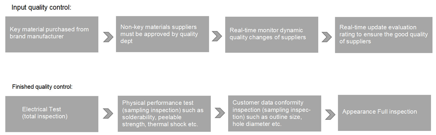
ABIS Quality Mission
The pass rate of incoming material above 99.9%, the number of mass rejection rates below 0.01%.
ABIS certified facilities control all key processes to eliminate all potential issues before producing.
ABIS utilizes advanced software to perform extensive DFM analysis on incoming data, and uses advanced quality control systems throughout the manufacturing process.
ABIS performs 100% visual and AOI inspection as well as performing electrical testing, high voltage testing, impedance control testing, micro-sectioning, thermal shock testing, solder testing, reliability testing, insulating resistance testing and ionic cleanliness testing.
Technology Road Map
|
Technology |
2019 |
2020 |
2021 |
|
Layer |
20 |
26 |
32 |
|
Max board thickness mm |
6 |
7 |
8 |
|
Min board thickness mm |
0.4 |
0.3 |
0.2 |
|
Max panel size/pcs size mm |
610*910 /580*850 |
620*1000 /580*950 |
620*1000 /580*950 |
|
Min Core thickness mm(without copper) |
0.075 |
0.05 |
0.05 |
|
Max copper thickness oz |
Inner layer :5oz; Out layer:6oz |
Inner Layer:6oz; Out layer:10oz |
Inner layer:6oz Out layer:10oz |
|
Min width/space μm |
75/75 |
65/65 |
50/50 |
|
Min Mec hole mm |
0.20 |
0.15 |
0.15 |
|
Min Laser drilling μm |
75 |
75 |
65 |
|
Aspect ratio |
13:1 |
16:1 |
16:1 |
|
MAX HDI Aspect ratio |
0.8:1 |
1:1 |
1:1 |
|
Registriation between layers(≥10L) μm |
125 |
100 |
76 |
|
Independence control tolerance |
±10% |
±8% |
±8% |
|
Back drill μm |
±75 |
±75 |
±75 |
|
Special process |
POFV(VIPPO)、High RF |
||
|
Surface finish |
ENIG、gold plating, HASL(HF), OSP, Immersion tin, Immersion silver |
||
Certificate


FAQ
Each Customer will have a sale to contact you. Our working hours: AM 9:00-PM 19:00(Beijing Time) from Monday to Friday. We will reply to your email as soon as quickly during our working time. And you also could contact our sales by cellphone if urgent.
Main Suppliers(FR4): Kingboard (Hong Kong), NanYa (Taiwan), and Shengyi (China), If others, please RFQ.
Our Quality Assuring Procedures as below:
a),Visual Inspection
b),Flying probe, fixture tool
c), Impedance control
d), Solder-ability detection
e), Digital metallograghic microscope
f),AOI (Automated Optical Inspection)
Generally 2-3 days for sample making. The lead time of mass production will depend on the order quantity and the season you place the order.
Our Quality Assuring Procedures as below:
a),Visual Inspection
b),Flying probe, fixture tool
c), Impedance control
d), Solder-ability detection
e), Digital metallograghic microscope
f),AOI (Automated Optical Inspection)
ISO9001, ISO14001,UL USA& USA Canada,IFA16949, SGS, RoHS report.
ABlS performs 100% visual and AOl inspection as well as performing electrical testing, high voltage testing, impedance control testing, micro-sectioning, thermal shock testing, solder testing, reliability testing, insulating resistance testing, ionic cleanliness testing and PCBA Functional testing.
Please send the details inquiry to us, such as the Item Number, Quantity for each item, Quality request, Logo, Payment Terms, Transport method, Discharge place, etc. We will make an accurate quotation for you as soon as possible.
On time delivery rate is more than 95%
a),24 hours fast turn for double side prototype PCB
b),48hours for 4-8 layers prototype PCB
c),1 hour for quotation
d),2 hours for engineer question/Complaint feedback
e),7-24 hours for technical support/order service/manufacturing operations