OEM 2 Layers Flexible ENIG Circuit Board

Basic Info
| Model No. | PCB-24 |
| Transport package | Vacuum Packing |
| Certification | UL, ISO9001&14001, SGS, RoHS, Ts16949 |
| Definitions | IPC Class2 |
| Minimum Space/Line | 0.075mm/3mil |
| HS Code | 85340090 |
| Origin | Made in China |
| Production Capacity | 720,000 M2/Year |
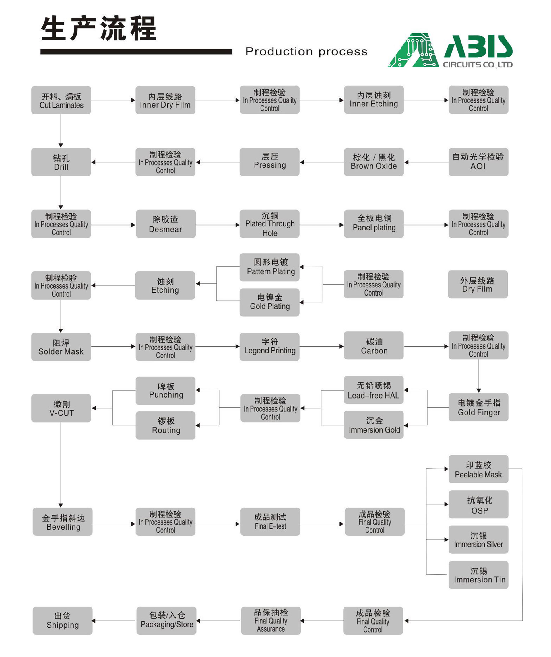
Production Process
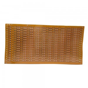
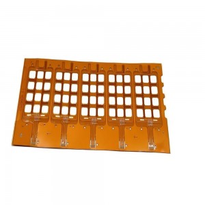
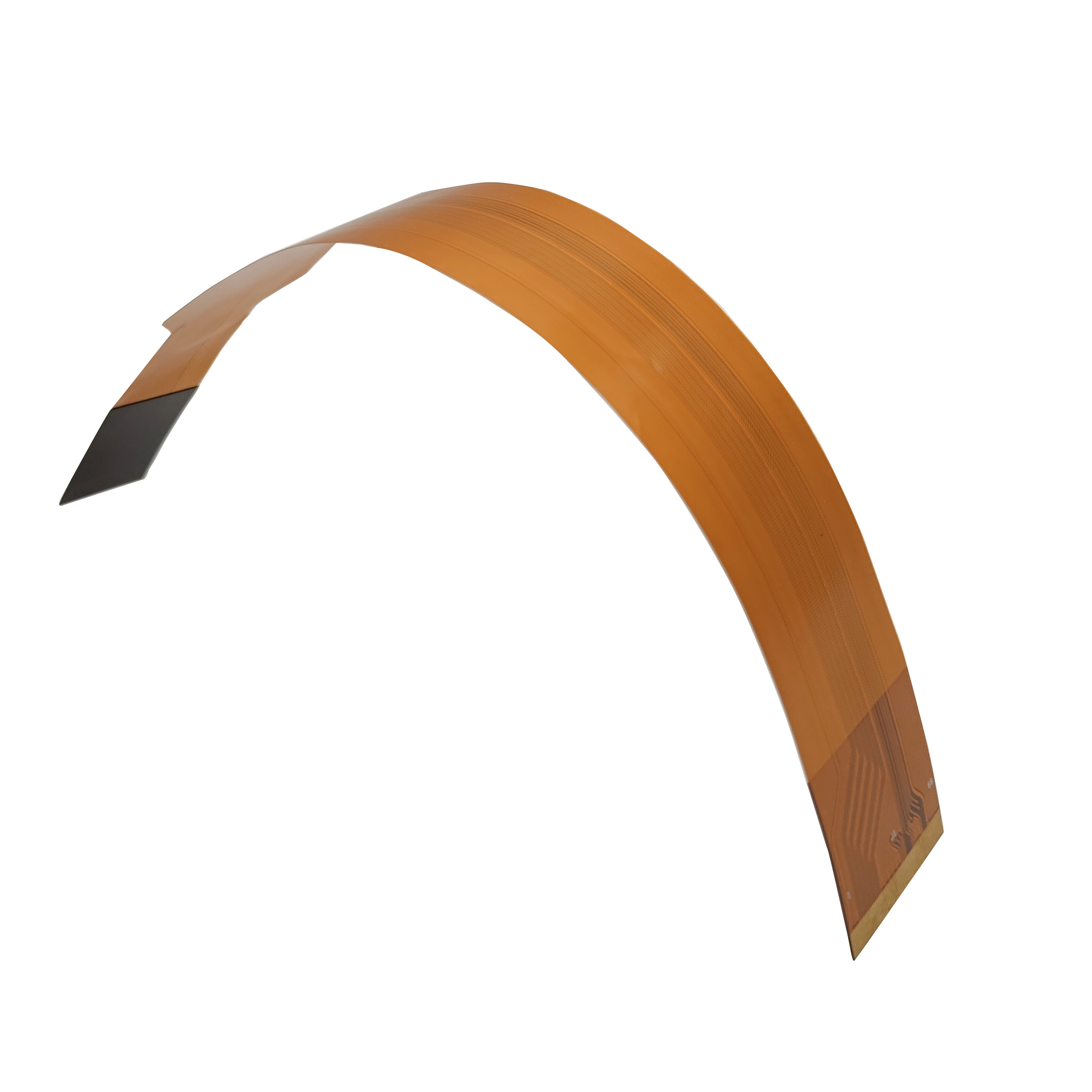
Flexible PCBs are an innovative type of printed circuit board that can bend, twist, and flex without damaging the circuitry. At our PCB manufacturing facility in Shenzhen, China, we offer a wide range of flexible PCBs, including our 2-layer flexible PCB model no. PCB-A24.
Our 2-layer flexible PCB has a dimension of 34.62mm*250.40mm and is made of PI (polyimide) base material, with a board thickness of 0.3mm and a copper thickness of 1.0oz.
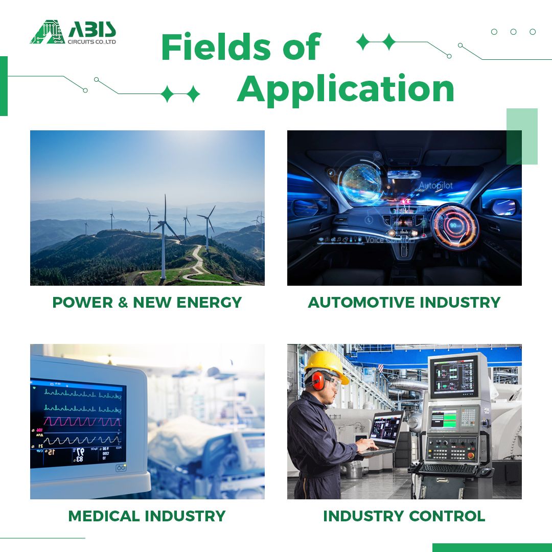
Our 2-layer flexible PCB is designed to meet IPC Class2 specifications, ensuring its reliability and high quality. It has been certified by UL, ISO9001&14001, SGS, RoHS, and Ts16949, making it suitable for a wide range of applications, including automotive, medical, industrial, and aerospace industries.
At our facility, we use the latest manufacturing technology and equipment to ensure that our flexible PCBs are produced with precision and efficiency. Our 2-layer flexible PCB is vacuum-packed for safe transportation and is available in bulk orders.
In summary, our 2-layer flexible PCB is a high-quality, reliable, and durable printed circuit board that can meet the most demanding industry standards. If you are looking for a flexible PCB for your project, look no further than our 2-layer flexible PCB model no. PCB-A24.
Technical & Capability
|
Item |
Speci. |
|
Layers |
1~8 |
|
Board Thickness |
0.1mm-0.2mm |
|
Substrate Material |
PI(0.5mil,1mil,2mil),PET(0.5mil,1mil) |
|
Conductive Medium |
Copper foil(1/3oz,1/2oz,1oz,2oz) Constantan Silver Paste Copper Ink |
|
Max Panel Size |
600mm×1200mm |
|
Min Hole Size |
0.1mm |
|
Min Line Width/Space |
3mil(0.075mm) |
|
Maximum imposition size (single & double panel) |
610mm*1200mm(Exposure limit) 250mm*35mm(only develop test samples) |
|
Maximum imposition size (single panel & double panel no PTH self-drying ink + UV light solid) |
610*1650mm |
|
Drilling Hole (Mechanical) |
17um--175um |
|
Finish Hole (Mechanical) |
0.10mm--6.30mm |
|
Diameter Tolerance (Mechanical) |
0.05mm |
|
Registration (Mechanical) |
0.075mm |
|
Aspect Ratio |
2:1(Minimum aperture 0.1mm) 5:1(Minimum aperture 0.2mm) 8:1(Minimum aperture 0.3mm) |
|
SMT Mini. Solder Mask Width |
0.075mm |
|
Mini. Solder Mask Clearance |
0.05mm |
|
Impedance Control Tolerance |
士10% |
|
Surface finish |
ENIG, HASL, Chem. Tin/Sn |
|
Solder mask/Protective Film |
PI(0.5mil,1mil,2mil)(Yellow, White, Black) PET(1mil,2mil) Solder mask (green, yellow, black...) |
|
Silkscreen |
Red/Yellow/Black/White |
|
Certificate |
UL, ISO 9001, ISO14001, IATF16949 |
|
Special Request |
Glue(3M467,3M468,3M9077,TESA8853...) |
|
Material Suppliers |
Shengyi, ITEQ, Taiyo, etc. |
|
Common Package |
Vacuum+Carton |
|
Monthly production capacity/m² |
60,000 m² |
How ABIS Dealing With Flexible PCB Issues?
The first thing we ensure is the right equipment to produce your board. Next, the staff experienced enough to handle the challenge of manufacturing flexible boards.
Opening a solder mask or overlay enough-different steps of the process might change how a flexible board looks. Etching and plating can adjust the shape of the PCB, which is why you should ensure that overlay openings are of suitable width.
Choose the materials carefully, also considering other things, such as size, weight, and reliability of the board.
Control appropriate proximity of solder joints and bending point – the solder joint should be at the required distance from the bending location. If you put them too close, delamination or broken solder pad may occur.
Control Solder pad spacing – ABIS ensuring there is enough space between the pads and the conductive traces adjacent to them, so that avoiding lamination loss.
Q/T Lead Time
| Category | Quickest Lead Time | Normal Lead Time |
| Double-sided | 24hrs | 120hrs |
| 4 Layers | 48hrs | 172hrs |
| 6 Layers | 72hrs | 192hrs |
| 8 Layers | 96hrs | 212hrs |
| 10 Layers | 120hrs | 268hrs |
| 12 Layers | 120hrs | 280hrs |
| 14 Layers | 144hrs | 292hrs |
| 16-20 Layers | Depends on the specific requirements | |
| Above 20 Layers | Depends on the specific requirements | |
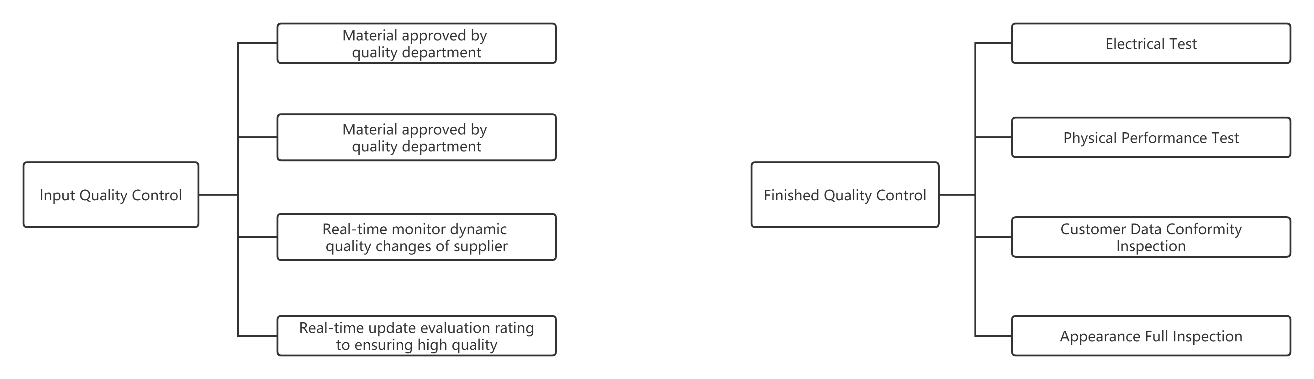
Quality Control
The pass rate of incoming material above 99.9%, the number of mass rejection rates below 0.01%.
ABIS certified facilities control all key processes to eliminate all potential issues before producing.
ABIS utilizes advanced software to perform extensive DFM analysis on incoming data, and uses advanced quality control systems throughout the manufacturing process.
ABIS performs 100% visual and AOI inspection as well as performing electrical testing, high voltage testing, impedance control testing, micro-sectioning, thermal shock testing, solder testing, reliability testing, insulating resistance testing and ionic cleanliness testing.
Certificate


FAQ
Our Quality Assuring Procedures as below:
a),Visual Inspection
b),Flying probe, fixture tool
c), Impedance control
d), Solder-ability detection
e), Digital metallograghic microscope
f),AOI (Automated Optical Inspection)
Bill of materials (BOM) detailing:
a), Manufacturers parts numbers,
b), Components suppliers' parts number (e.g. Digi-key, Mouser, RS )
c), PCBA sample photos if possible.
d), Quantity
A: It's no problem. If you're a small wholesaler, we would like to grow up with you together.
A: Generally 2-3 days for sample making. The lead time of mass production will depend on the order quantity and the season you place the order.
No, we can't accpet picture files, if you no not have gerber file, can you send us sample to copy it.
PCB&PCBA Copy Process:
A: Each Customer will have a sale to contact with you. Our working hours: AM 9:00-PM 19:00(Beijing Time) from Monday to Friday. We will reply to your email as soon as quickly during our working time. And you also could contact our sales by cellphone if urgent.
a),1 Hour quotation
b),2 hours of complaint feedback
c),7*24 hour technical support
d),7*24 order service
e),7*24 hour delivery
f),7*24 production run
A: yes, We have a professional drawing engineers' team that you can trust.
On time delivery rate is more than 95%
a),24 hours fast turn for double side prototype PCB
b),48hours for 4-8 layers prototype PCB
c),1 hour for quotation
d),2 hours for engineer question/Complaint feedback
e),7-24 hours for technical support/order service/manufacturing operations
ABlS performs 100% visual and AOl inspection as well as performing electrical testing, high voltage testing, impedancecontrol testing, micro-sectioning, thermal shock testing, solder testing, reliability testing, insulating resistance testing, ionic cleanliness testing and PCBA Functional testing.
ABIS's Main Industries: Industrial Control, Telecommunication, Automotive Products and Medical. ABIS's Main Market: 90% International Market(40%-50% for USA, 35% for Europe, 5% for Russia and 5%-10% for East Asia) and 10% Domestic Market.