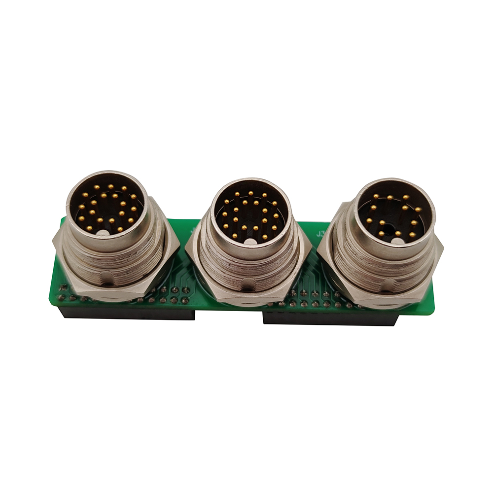
Aviation Connector PCB Assembly Module

Basic Info
| Model No. | PCBA-A30 |
| Assembly method | Post Welding |
| Transport package | Anti-static Packaging |
| Certification | UL, ISO9001&14001, SGS, RoHS, Ts16949 |
| Definitions | IPC Class2 |
| Minimum Space/Line | 0.075mm/3mil |
| Application | Signal transmission |
| Origin | Made in China |
| Production Capacity | 720,000 M2/Year |
Product Description

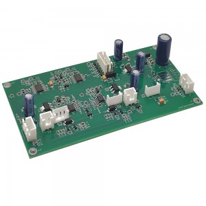
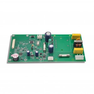
As a leading PCB and PCBA manufacturer based in Shenzhen, China, ABIS Circuits is committed to providing high-quality products for a wide range of applications. One of our latest offerings is the PCBA-A30, a 2-layer Printed Circuit Board (PCB) designed for signal transmission.
The PCBA-A30 PCB has a compact size, with dimensions of 69mm*20mm and a board thickness of 1.6mm. The base material used in the PCB is FR4, a commonly used flame-retardant material in the electronics industry. The PCB's surface finish is HASL-LF, which stands for Hot Air Solder Leveling with Lead-Free (LF) finish. This finish is environmentally friendly and provides a smooth and even surface for component mounting.
The PCBA-A30 PCB is assembled using Post Welding, a process where components are first inserted into holes in the PCB, and then the leads are soldered onto the board's pads. This method is commonly used for components that are too large to be mounted using Surface Mount Technology (SMT) or for components that require a high degree of mechanical strength. The use of Post Welding ensures that all components are securely mounted on the PCB, providing a stable and reliable board for signal transmission.
The PCBA-A30 PCB is designed for signal transmission applications. It is an ideal choice for applications where compact size and reliability are critical, such as in telecommunications, data communication, and control systems.
At ABIS Circuits, we are committed to providing high-quality PCBs and PCBA assemblies to our customers. Our manufacturing processes adhere to industry standards, and we use the latest technology and equipment to ensure our products meet the highest standards of quality and reliability. The PCBA-A30 is an excellent example of the type of high-quality products we produce, and we are confident that it will meet the needs of our customers for signal transmission applications.
In conclusion, the PCBA-A30 is a high-quality PCB designed for signal transmission applications. With its compact size, HASL-LF surface finish, Post Welding assembly, and anti-static packaging, it provides a reliable and stable solution for signal transmission. As a leading PCB and PCBA manufacturer in Shenzhen, China, ABIS Circuits is committed to providing the highest quality products and services to our customers.
Q/T Lead Time
| Category | Quickest Lead Time | Normal Lead Time |
| Double-sided | 24hrs | 120hrs |
| 4 Layers | 48hrs | 172hrs |
| 6 Layers | 72hrs | 192hrs |
| 8 Layers | 96hrs | 212hrs |
| 10 Layers | 120hrs | 268hrs |
| 12 Layers | 120hrs | 280hrs |
| 14 Layers | 144hrs | 292hrs |
| 16-20 Layers | Depends on the specific requirements | |
| Above 20 Layers | Depends on the specific requirements | |
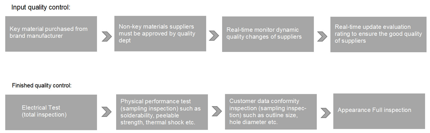
Quality Control
FAQ
A: We usually quote 1 hour after we get your inquiry. If you are very urgent, please call us or tell us in your email.
A: Free samples depend on your order quantity.
A: It's no problem. If you're a small wholesaler, we would like to grow up with you together.
A: Generally 2-3 days for sample making. The lead time of mass production will depend on the order quantity and the season you place the order.
A: Please send the details inquiry to us, such as the Item Number, Quantity for each item, Quality request, Logo, Payment Terms, Transport method, Discharge place, etc. We will make an accurate quotation for you as soon as possible.
A: Each Customer will have a sale to contact with you. Our working hours: AM 9:00-PM 19:00(Beijing Time) from Monday to Friday. We will reply to your email as soon as quickly during our working time. And you also could contact our sales by cellphone if urgent.
A: Yes, we are pleased to supply module samples to test and check the quality, mixed sample order is available. Please note buyer should pay for the shipping cost.
A: yes, We have a professional drawing engineers' team that you can trust.
A: Yes, we ensure that each piece of PCB, and PCBA will be tested before shipment, and we ensure the goods we sent with good quality.
A: We suggest you use DHL, UPS, FedEx, and TNT forwarder.
A: By T/T, Paypal, Western Union, etc.