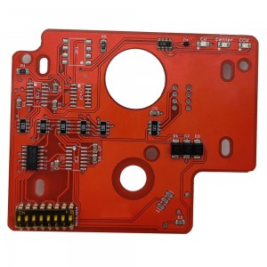
Full-Service PCB Assembly Solutions PCBA board for Industrial electronics


Manufacturing info
| Model No. | PCB-A43 |
| Assembly method | SMT |
| Transport package | Anti-static Packaging |
| Certification | UL, ISO9001&14001, SGS, RoHS, Ts16949 |
| Definitions | IPC Class2 |
| Minimum Space/Line | 0.075mm/3mil |
| Application | Communication |
| Origin | Made in China |
| Production Capacity | 720,000 M2/Year |
Product Description
PCBA Projects Introduction
ABIS CIRCUITS Company deliver services, not only products. We offer solutions, not only goods.
From the PCB production, the components purchasing to the components assemble. Includes:
PCB Custom
PCB drawing / design according to your schematic diagram
PCB manufacturing
Component sourcing
PCB Assemble
PCBA 100% test
PCBA Capabilities
| 1 | SMT assembly including BGA assembly |
| 2 | Accepted SMD chips: 0204, BGA, QFP, QFN, TSOP |
| 3 | Component height: 0.2-25mm |
| 4 | Min packing: 0204 |
| 5 | Min distance among BGA : 0.25-2.0mm |
| 6 | Min BGA size: 0.1-0.63mm |
| 7 | Min QFP space: 0.35mm |
| 8 | Min assembly size: (X*Y): 50*30mm |
| 9 | Max assembly size: (X*Y): 350*550mm |
| 10 | Pick-placement precision: ±0.01mm |
| 11 | Placement capability: 0805, 0603, 0402 |
| 12 | High pin count press fit available |
| 13 | SMT capacity per day: 80,000 points |
Capability - SMT
|
Lines |
9(5 Yamaha,4KME) |
|
Capacity |
52 million placements per month |
|
Max Board Size |
457*356mm.(18”X14”) |
|
Min Component size |
0201-54 sq.mm.(0.084 sq.inch),long connector,CSP,BGA,QFP |
|
Speed |
0.15 sec/chip,0.7 sec/QFP |
Capability - PTH
|
Lines |
2 |
|
Max board width |
400 mm |
|
Type |
Dual wave |
|
Pbs status |
Lead-free line support |
|
Max temp |
399 degree C |
|
Spray flux |
add-on |
|
Pre-heat |
3 |
What is DIP
dual inline-pin package,Refers to integrated circuit chips packaged in dual-in-line form. Most small and medium-sized integrated circuits use this package.
Our DIP Line
5 DIP Hand Soldering Line
ABIS have 5 DIP Hand Soldering Line to finish projects better for our clients.
Process Engineer Responsibility
Our engineers will check the conditions on the production line and give a feedback of problem.
Quality Control
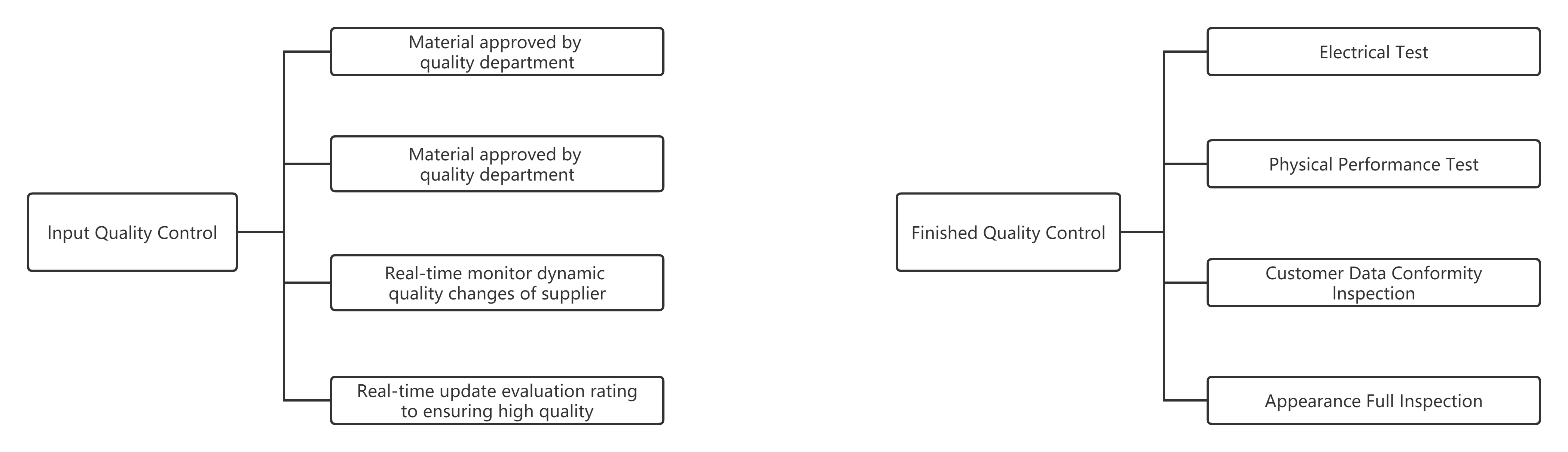
| AOI Testing | Checks for solder pasteChecks for components down to 0201
Checks for missing components, offset, incorrect parts, polarity |
| X-Ray Inspection | X-Ray provides high-resolution inspection of:BGAs/Micro BGAs/Chip scale packages /Bare boards |
| In-Circuit Testing | In-Circuit Testing is commonly used in conjunction with AOI minimizing functional defects caused by component problems. |
| Power-up Test | Advanced Function TestFlash Device Programming
Functional testing |
Certificate


FAQ
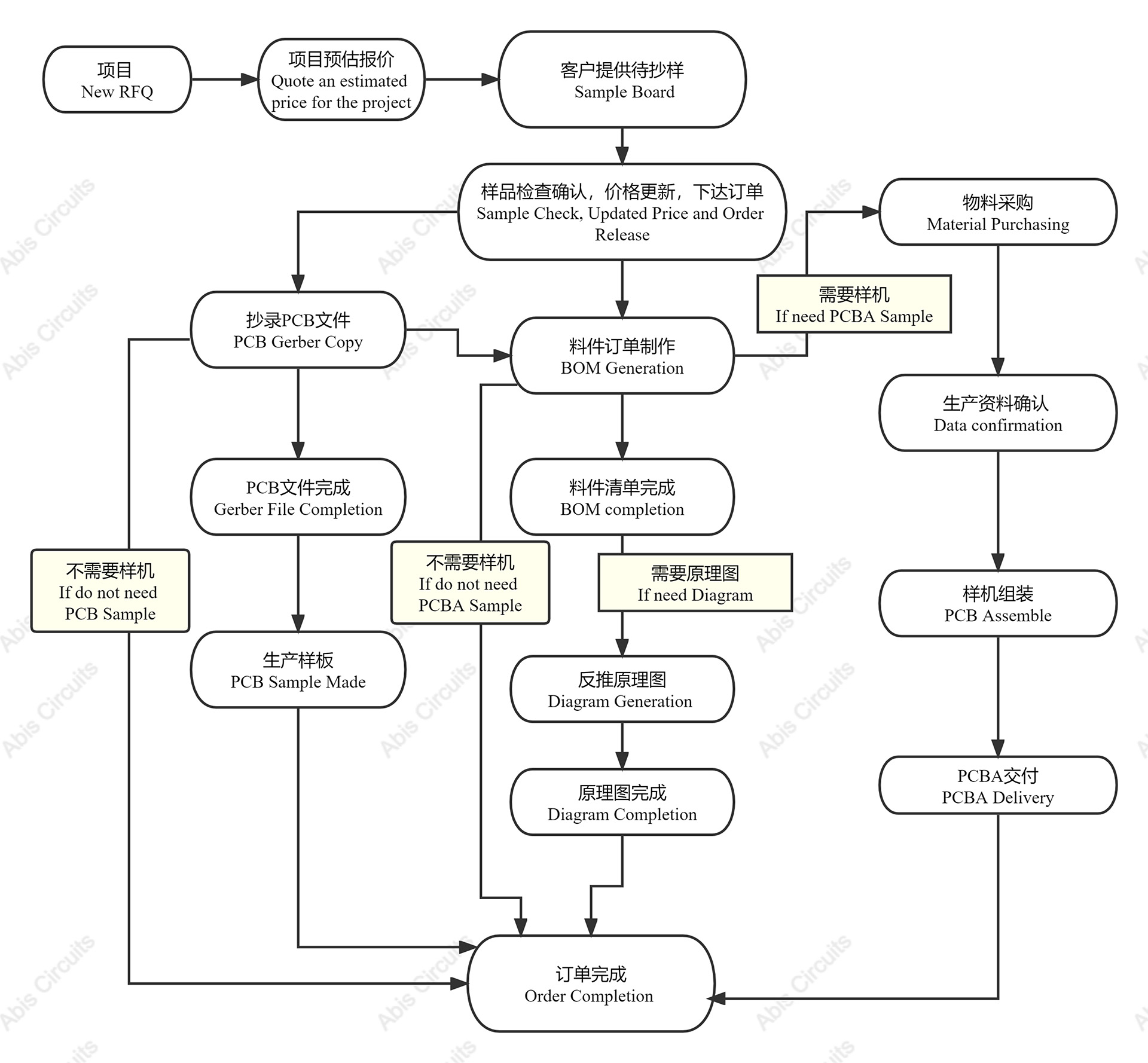
No, we can't accpet picture files, if you no not have gerber file, can you send us sample to copy it.
PCB&PCBA Copy Process:
Yes, PCBs can be assembled by hand, but it is a time-consuming and error-prone process. Automated assembly using pick-and-place machines is the preferred method for most PCBs.
A PCB is a board with copper tracks and pads that connect electronic components. PCBA refers to the assembly of components onto a PCB to create a functioning electronic device.
Solder paste is used to temporarily hold electronic components in place before they are permanently attached to the PCB during the reflow soldering process.
| Production capacity of hot-sale products | |
| Double Side/Multilayer PCB Workshop | Aluminum PCB Workshop |
| Technical Capability | Technical Capability |
| Raw materials: CEM-1, CEM-3, FR-4(High TG), Rogers, TELFON | Raw materials: Aluminum base, Copper base |
| Layer: 1 layer to 20 Layers | Layer: 1 layer and 2 Layers |
| Min.line width/space: 3mil/3mil(0.075mm/0.075mm) | Min.line width/space: 4mil/4mil(0.1mm/0.1mm) |
| Min.Hole size: 0.1mm(dirilling hole) | Min. Hole size: 12mil(0.3mm) |
| Max. Board size: 1200mm* 600mm | Max.Board size: 1200mm* 560mm(47in* 22in) |
| Finished board thickness: 0.2mm- 6.0mm | Finished board thickness: 0.3~ 5mm |
| Copper foil thickness: 18um~280um(0.5oz~8oz) | Copper foil thickness: 35um~210um(1oz~6oz) |
| NPTH Hole Tolerance: +/-0.075mm, PTH hole Tolerance: +/-0.05mm | Hole position tolerance: +/-0.05mm |
| Outline Tolerance: +/-0.13mm | Routing outline tolerance: +/ 0.15mm; punching outline tolerance:+/ 0.1mm |
| Surface finished: Lead-free HASL, immersion gold(ENIG), immersion silver, OSP, gold plating, gold finger, Carbon INK. | Surface finished: Lead free HASL, immersion gold(ENIG), immersion silver, OSP etc |
| Impedance control tolerance: +/-10% | Remain thickness tolerance: +/-0.1mm |
| Production capability: 50,000 s.q.m/month | MC PCB Production capability: 10,000 s.q.m/month |
Our Quality Assuring Procedures as below:
a),Visual Inspection
b),Flying probe, fixture tool
c), Impedance control
d), Solder-ability detection
e), Digital metallograghic microscope
f),AOI (Automated Optical Inspection)
Bill of materials (BOM) detailing:
a), Manufacturers parts numbers,
b), Components suppliers' parts number (e.g. Digi-key, Mouser, RS )
c), PCBA sample photos if possible.
d), Quantity
ABIS has no MOQ requirements for either PCB or PCBA.
ABlS performs 100% visual and AOl inspection as well as performing electrical testing, high voltage testing, impedancecontrol testing, micro-sectioning, thermal shock testing, solder testing, reliability testing, insulating resistance testing, ionic cleanliness testing and PCBA Functional testing.
·With ABIS, customers significantly and effectively reduce their global procurement costs. Behind each service provided by ABIS, is hidden a cost-saving for customers.
. We have two shops together, one is for prototype, quick turn, and small volume making. The other is for mass production also for the HDI board, with highly skilled professional employees, for high-quality products with competitive prices and on-time delivery.
. We provide very professional sales, technical and logistic support, on a worldwide basis with 24 hours of complaint feedback.