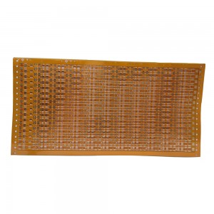
Customized flexible FPC High Frequency Anti-metal Electronic Tag


Basic Info
| Model No. | PCB-A37 |
| Transport package | Vacuum Packing |
| Certification | UL, ISO9001&14001, SGS, RoHS, Ts16949 |
| Definitions | IPC Class2 |
| Minimum Space/Line | 0.075mm/3mil |
| HS Code | 85340090 |
| Origin | Made in China |
| Production Capacity | 720,000 M2/Year |
Product Description
Flexible printed circuit board overview
Definition
Flexible PCB – Flexible Printed Circuit, referred to as FPC.
A flexible printed circuit can be defined as an outline of conductive traces bonded on a flexible substrate. It is made into conductor circuit patterns using light pattern expose transfer and etching processes on the surface of a flexible substrate.
Characteristics
Flex circuits widely used in mobile phones, cameras and smart wearable.
It can better fit wiring capability in spaces than the traditional rigid boards.Flexible circuit boards also have better resistance to high temperatures, shock and vibrations. it has good performance with design challenges such as: unavoidable crossovers, specific impedance requirements, elimination of cross talk, additional shielding and high component density.
Classify
Single-sided flex PCB
Single-sided flex with dual access
Double-sided flex PCB
Multi-layer flex PCB
Technical & Capability
|
Item |
Speci. |
|
Layers |
1~8 |
|
Board Thickness |
0.1mm-0.2mm |
|
Substrate Material |
PI(0.5mil,1mil,2mil),PET(0.5mil,1mil) |
|
Conductive Medium |
Copper foil(1/3oz,1/2oz,1oz,2oz) Constantan Silver Paste Copper Ink |
|
Max Panel Size |
600mm×1200mm |
|
Min Hole Size |
0.1mm |
|
Min Line Width/Space |
3mil(0.075mm) |
|
Maximum imposition size (single & double panel) |
610mm*1200mm(Exposure limit) 250mm*35mm(only develop test samples) |
|
Maximum imposition size (single panel & double panel no PTH self-drying ink + UV light solid) |
610*1650mm |
|
Drilling Hole (Mechanical) |
17um--175um |
|
Finish Hole (Mechanical) |
0.10mm--6.30mm |
|
Diameter Tolerance (Mechanical) |
0.05mm |
|
Registration (Mechanical) |
0.075mm |
|
Aspect Ratio |
2:1(Minimum aperture 0.1mm) 5:1(Minimum aperture 0.2mm) 8:1(Minimum aperture 0.3mm) |
|
SMT Mini. Solder Mask Width |
0.075mm |
|
Mini. Solder Mask Clearance |
0.05mm |
|
Impedance Control Tolerance |
士10% |
|
Surface finish |
ENIG, HASL, Chem. Tin/Sn |
|
Solder mask/Protective Film |
PI(0.5mil,1mil,2mil)(Yellow, White, Black) PET(1mil,2mil) Solder mask (green, yellow, black...) |
|
Silkscreen |
Red/Yellow/Black/White |
|
Certificate |
UL, ISO 9001, ISO14001, IATF16949 |
|
Special Request |
Glue(3M467,3M468,3M9077,TESA8853...) |
|
Material Suppliers |
Shengyi, ITEQ, Taiyo, etc. |
|
Common Package |
Vacuum+Carton |
|
Monthly production capacity/m² |
60,000 m² |
Q/T Lead Time
| Category | Quickest Lead Time | Normal Lead Time |
| Double-sided | 24hrs | 120hrs |
| 4 Layers | 48hrs | 172hrs |
| 6 Layers | 72hrs | 192hrs |
| 8 Layers | 96hrs | 212hrs |
| 10 Layers | 120hrs | 268hrs |
| 12 Layers | 120hrs | 280hrs |
| 14 Layers | 144hrs | 292hrs |
| 16-20 Layers | Depends on the specific requirements | |
| Above 20 Layers | Depends on the specific requirements | |
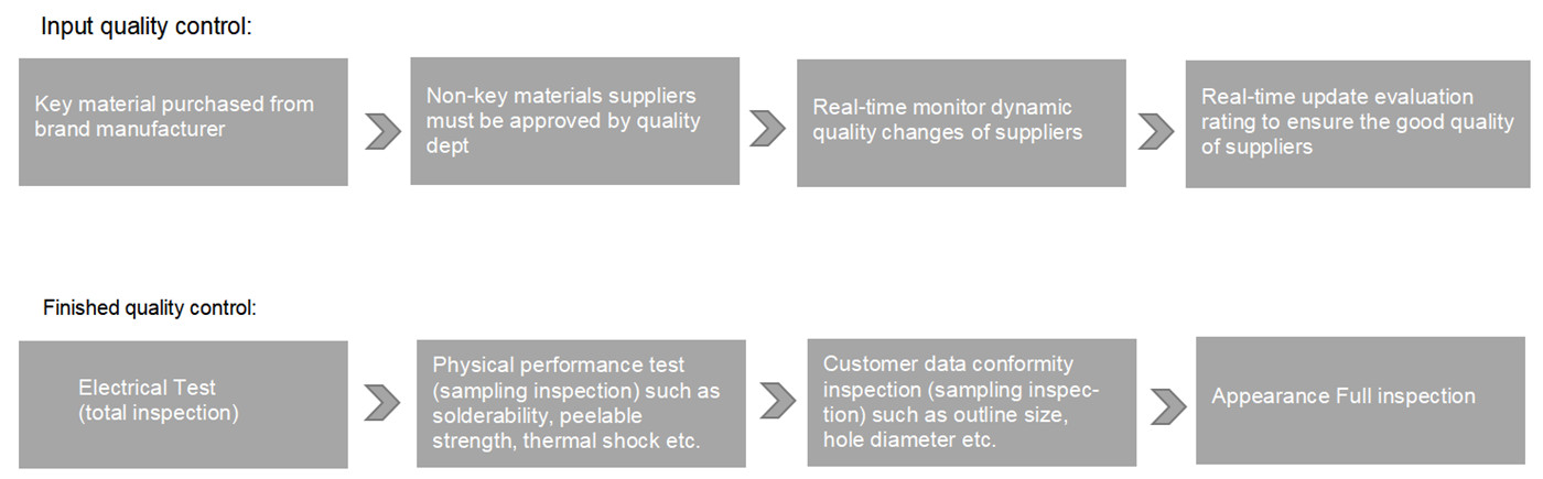
Quality Control
Certificate


FAQ
A: We usually quote 1 hour after we get your inquiry. If you are very urgent, please call us or tell us in your email.
Bill of materials (BOM) detailing:
a), Manufacturers parts numbers,
b), Components suppliers' parts number (e.g. Digi-key, Mouser, RS )
c), PCBA sample photos if possible.
d), Quantity
A: It's no problem. If you're a small wholesaler, we would like to grow up with you together.
A: Generally 2-3 days for sample making. The lead time of mass production will depend on the order quantity and the season you place the order.
A: Please send the details inquiry to us, such as the Item Number, Quantity for each item, Quality request, Logo, Payment Terms, Transport method, Discharge place, etc. We will make an accurate quotation for you as soon as possible.
A: Each Customer will have a sale to contact with you. Our working hours: AM 9:00-PM 19:00(Beijing Time) from Monday to Friday. We will reply to your email as soon as quickly during our working time. And you also could contact our sales by cellphone if urgent.
A: Yes, we are pleased to supply module samples to test and check the quality, mixed sample order is available. Please note buyer should pay for the shipping cost.
A: yes, We have a professional drawing engineers' team that you can trust.
A: Yes, we ensure that each piece of PCB, and PCBA will be tested before shipment, and we ensure the goods we sent with good quality.
ABlS performs 100% visual and AOl inspection as well as performing electrical testing, high voltage testing, impedancecontrol testing, micro-sectioning, thermal shock testing, solder testing, reliability testing, insulating resistance testing, ionic cleanliness testing and PCBA Functional testing.
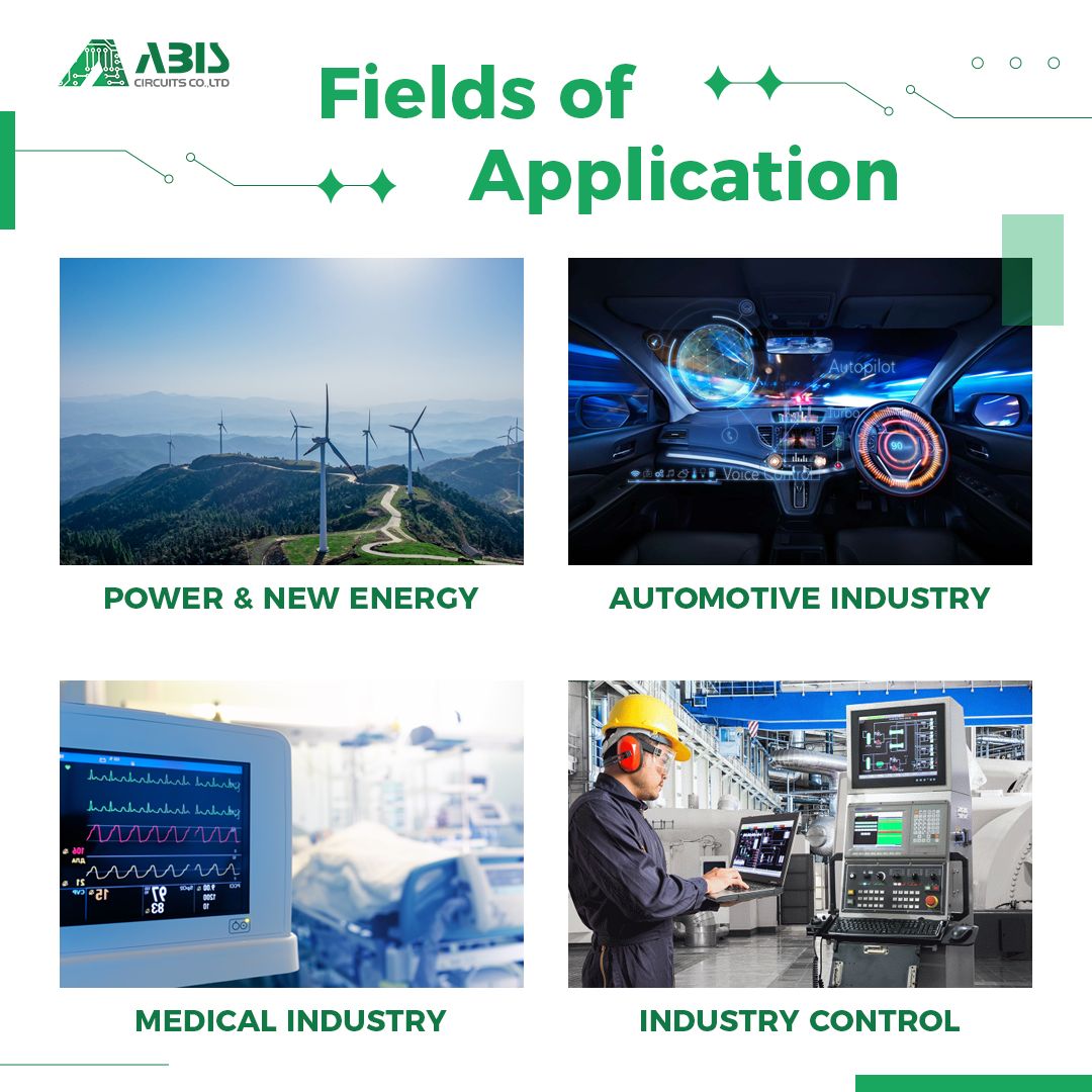
ABIS's Main Industries: Industrial Control, Telecommunication, Automotive Products and Medical. ABIS's Main Market: 90% International Market(40%-50% for USA, 35% for Europe, 5% for Russia and 5%-10% for East Asia) and 10% Domestic Market.