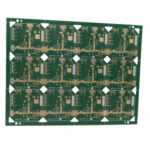
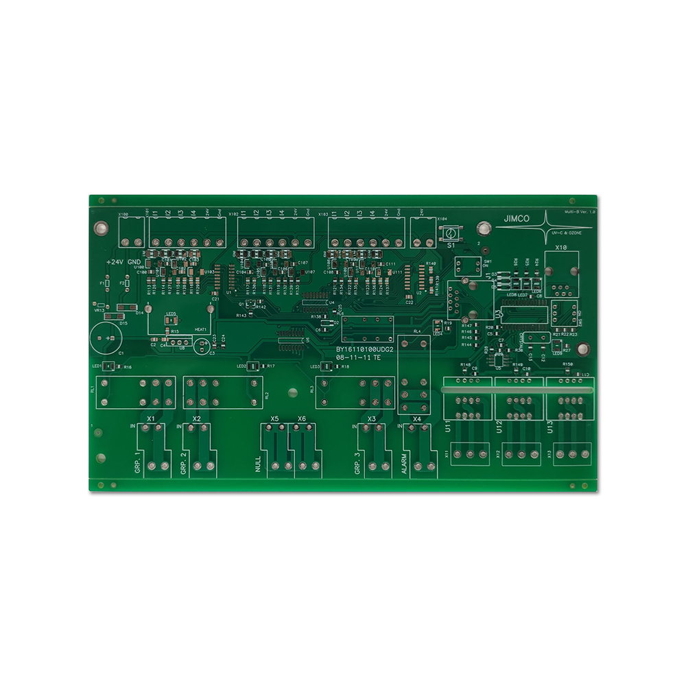
4 Layers Wide line 4.0oz Copper ENIG PCB

Basic Info
| Model No. | PCB-A23 |
| Transport package | Vacuum Packing |
| Certification | UL, ISO9001&14001, SGS, RoHS, Ts16949 |
| Definitions | IPC Class2 |
| Minimum Space/Line | 0.075mm/3mil |
| HS Code | 85340090 |
| Origin | Made in China |
| Production Capacity | 720,000 M2/Year |
Product Description
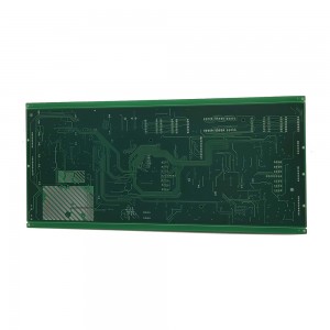
Our PCB-A23 is a high-quality 4-layer printed circuit board (PCB) designed for a wide range of electronic applications. This heavy copper PCB is constructed using FR4 base material, with a board thickness of 1.6mm, and a copper thickness of 4.0oz. With a dimension of 95mm*160mm, this PCB is the perfect choice for your next project.
To ensure maximum durability and reliability, our PCB-A23 features an ENIG surface finish. This surface finish provides excellent corrosion resistance, making it ideal for use in harsh environments. The ENIG finish also provides a flat, even surface, ensuring excellent solderability for your components.
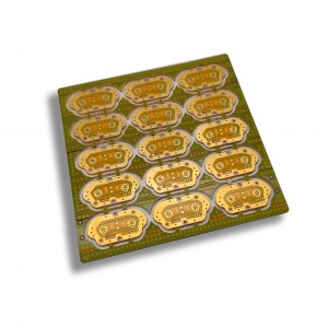
Our PCB-A23 is a heavy copper PCB that is designed to carry high current and withstand high temperatures. With a copper thickness of 4.0oz, this PCB is perfect for use in applications that require high power or high heat dissipation.
At our manufacturing facility in Shenzhen, China, we take quality and reliability seriously. That's why our PCB-A23 comes with UL, ISO9001&14001, SGS, RoHS, and Ts16949 certifications. You can be confident that our PCBs meet the highest industry standards.
Our PCB-A23 is proudly made in China, using the latest manufacturing techniques and equipment. We take pride in producing high-quality PCBs that meet the needs of our customers.
In summary, our 4 Layers Wide line 4.0oz Copper ENIG PCB - PCB-A23 is a heavy copper PCB that is designed to meet the needs of a wide range of electronic applications. With its high-quality construction, ENIG surface finish, and certifications, you can be confident that our PCBs are reliable and durable. So why wait? Order your PCB-A23 today!
Q/T Lead Time
| Category | Quickest Lead Time | Normal Lead Time |
| Double-sided | 24hrs | 120hrs |
| 4 Layers | 48hrs | 172hrs |
| 6 Layers | 72hrs | 192hrs |
| 8 Layers | 96hrs | 212hrs |
| 10 Layers | 120hrs | 268hrs |
| 12 Layers | 120hrs | 280hrs |
| 14 Layers | 144hrs | 292hrs |
| 16-20 Layers | Depends on the specific requirements | |
| Above 20 Layers | Depends on the specific requirements | |
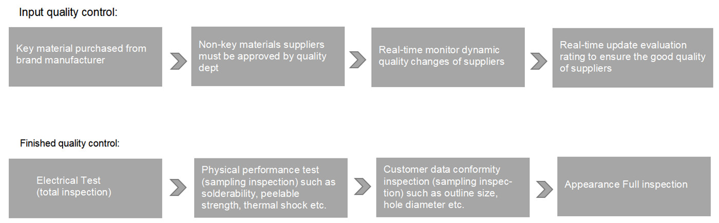
ABIS' move to control FR4 PCBS
Hole Preparation
Removing debris carefully & adjusting drill machine parameters: before plating through with copper, ABIS pays high attention to all holes on an FR4 PCB treated to remove debris, surface irregularities, and epoxy smear, the clean holes ensure the plating successfully adheres to the hole walls. also, early in the process, drill machine parameters are adjusted accurately.
Surface Preparation
Deburring carefully: our experienced tech workers will be aware ahead of time that the only way to avoid a bad outcome is to anticipate the need for special handling and to take the appropriate steps to be sure that the process is done carefully and correctly.
Thermal Expansion Rates
Accustomed to dealing with the various materials, ABIS will be able to analyze the combination to be sure that it is appropriate. then keeping the long-term reliability of the CTE (coefficient of thermal expansion), with the lower CTE, the less likely the plated through holes are to fail from repeated flexing of the copper which forms the internal layer interconnections.
Scaling
ABIS control the circuitry is scaled-up by known percentages in anticipation of this loss so that the layers will return to their as-designed dimensions after the lamination cycle is complete. also, using the laminate manufacturer’s baseline scaling recommendations in combination with in-house statistical process control data, to dial-in scale factors that will be consistent over time within that particular manufacturing environment.
Machining
When the time comes to build your PCB, ABIS be sure that you choose has the right equipment and experience to produce it correctly on the first try.
ABIS Quality Mission
The pass rate of incoming material above 99.9%, the number of mass rejection rates below 0.01%.
ABIS certified facilities control all key processes to eliminate all potential issues before producing.
ABIS utilizes advanced software to perform extensive DFM analysis on incoming data, and uses advanced quality control systems throughout the manufacturing process.
ABIS performs 100% visual and AOI inspection as well as performing electrical testing, high voltage testing, impedance control testing, micro-sectioning, thermal shock testing, solder testing, reliability testing, insulating resistance testing and ionic cleanliness testing.
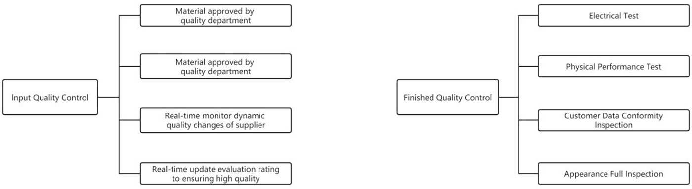
Quality Control
Certificate


FAQ
A: We usually quote 1 hour after we get your inquiry. If you are very urgent, please call us or tell us in your email.
A: Free samples depend on your order quantity.
A: It's no problem. If you're a small wholesaler, we would like to grow up with you together.
A: Generally 2-3 days for sample making. The lead time of mass production will depend on the order quantity and the season you place the order.
A: Please send the details inquiry to us, such as the Item Number, Quantity for each item, Quality request, Logo, Payment Terms, Transport method, Discharge place, etc. We will make an accurate quotation for you as soon as possible.
A: Each Customer will have a sale to contact with you. Our working hours: AM 9:00-PM 19:00(Beijing Time) from Monday to Friday. We will reply to your email as soon as quickly during our working time. And you also could contact our sales by cellphone if urgent.
A: Yes, we are pleased to supply module samples to test and check the quality, mixed sample order is available. Please note buyer should pay for the shipping cost.
A: yes, We have a professional drawing engineers' team that you can trust.
A: Yes, we ensure that each piece of PCB, and PCBA will be tested before shipment, and we ensure the goods we sent with good quality.
A: We suggest you use DHL, UPS, FedEx, and TNT forwarder.
A: By T/T, Paypal, Western Union, etc.