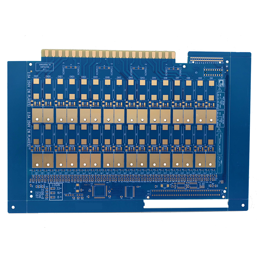
4oz Multilayer FR4 PCB Board in ENIG used in Energy Industry with IPC Class 3

Manufacturing info
| Model No. | PCB-A9 |
| Transport package | Vacuum Packing |
| Certification | UL,ISO9001&ISO14001,RoHS |
| Application | Consumer electronics |
| Minimum Space/Line | 0.075mm/3mil |
| Production Capacity | 50,000 s.q.m/month |
| HS Code | 853400900 |
| Origin | Made in China |
Product Description
FR4 PCB Introduction
Definition
FR means “flame-retardant,” FR-4 (or FR4) is a NEMA grade designation for glass-reinforced epoxy laminate material, a composite material composed of woven fiberglass cloth with an epoxy resin binder that makes it an ideal substrate for electronic components on a printed circuit board.
Pros and Cons of FR4 PCB
FR-4 material is so popular because of its many wondrous qualities that can benefit printed circuit boards. In addition to being affordable and easy to work with, it is an electrical insulator with very high dielectric strength. Plus, it's durable, moisture-resistant, temperature-resistant and lightweight.
FR-4 is a widely relevant material, popular mostly for its low cost and relative mechanical and electrical stability. While this material features extensive benefits and is available in a variety of thicknesses and sizes, it isn't the best choice for every application, especially high-frequency applications like RF and microwave designs.
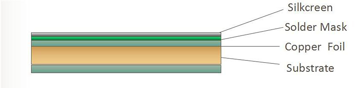
Multi-layer PCB Structure
Multilayer PCBs further increases the complexity and density of PCB designs by adding additional layers beyond the top and bottom layers seen in double sided boards. Multilayer PCBs are built by laminating the various layers. The inner-layers, normally double-sided circuit boards, are stacked together, with insulating layers in between and between the copper-foil for the outer-layers. Holes drilled through the board (vias) will make connections with the different layers of the board.
Technical & Capability
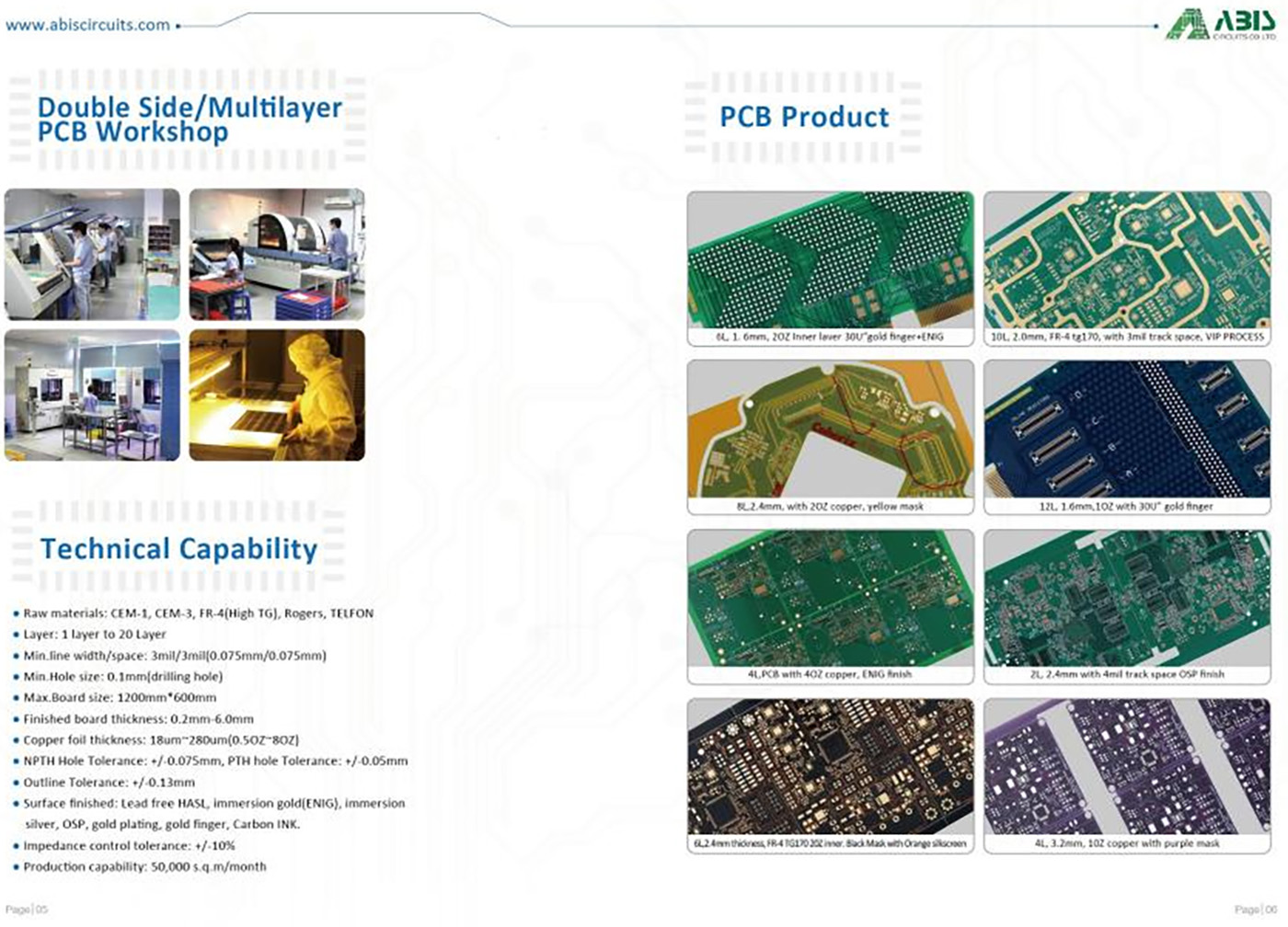
| Item | Production Capacity |
| Layer Counts | 1-20 layers |
| Material | FR-4, CEM-1/CEM-3, PI, High Tg, Rogers, PTEF, Alu/Cu Base, etc |
| Board thickness | 0.10mm-8.00mm |
| Maximum Size | 600mmX1200mm |
| Board Outline Tolerance | +0.10mm |
| Thickness Tolerance(t≥0.8mm) | ±8% |
| Thickness Tolerance(t<0.8mm) | ±10% |
| Insulation Layer Thickness | 0.075mm--5.00mm |
| Minimum Line | 0.075mm |
| Minimum Space | 0.075mm |
| Out Layer Copper Thickness | 18um--350um |
| Inner Layer Copper Thickness | 17um--175um |
| Drilling Hole(Mechanical) | 0.15mm--6.35mm |
| Finish Hole(Mechanical) | 0.10mm-6.30mm |
| Diameter Tolerance(Mechanical) | 0.05mm |
| Registration(Mechanical) | 0.075mm |
| Aspect Ratio | 16:1 |
| Solder Mask Type | LPI |
| SMT Mini.Solder Mask Width | 0.075mm |
| Mini. Solder Mask Clearance | 0.05mm |
| Plug Hole Diameter | 0.25mm--0.60mm |
| Impedance control Tolerance | ±10% |
| Surface finish/treatment | HASL, ENIG, Chem, Tin, Flash Gold, OSP, Gold Finger |
Q/T Lead Time
| Category | Quickest Lead Time | Normal Lead Time |
| Double-sided | 24hrs | 120hrs |
| 4 Layers | 48hrs | 172hrs |
| 6 Layers | 72hrs | 192hrs |
| 8 Layers | 96hrs | 212hrs |
| 10 Layers | 120hrs | 268hrs |
| 12 Layers | 120hrs | 280hrs |
| 14 Layers | 144hrs | 292hrs |
| 16-20 Layers | Depends on the specific requirements | |
| Above 20 Layers | Depends on the specific requirements | |
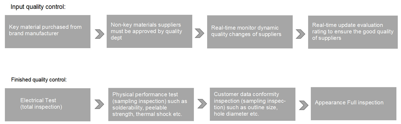
ABIS' move to control FR4 PCBS
Hole Preparation
Removing debris carefully & adjusting drill machine parameters: before plating through with copper, ABIS pays high attention to all holes on an FR4 PCB treated to remove debris, surface irregularities, and epoxy smear, the clean holes ensure the plating successfully adheres to the hole walls. also, early in the process, drill machine parameters are adjusted accurately.
Surface Preparation
Deburring carefully: our experienced tech workers will be aware ahead of time that the only way to avoid a bad outcome is to anticipate the need for special handling and to take the appropriate steps to be sure that the process is done carefully and correctly.
Thermal Expansion Rates
Accustomed to dealing with the various materials, ABIS will be able to analyze the combination to be sure that it is appropriate. then keeping the long-term reliability of the CTE (coefficient of thermal expansion), with the lower CTE, the less likely the plated through holes are to fail from repeated flexing of the copper which forms the internal layer interconnections.
Scaling
ABIS control the circuitry is scaled-up by known percentages in anticipation of this loss so that the layers will return to their as-designed dimensions after the lamination cycle is complete. also, using the laminate manufacturer’s baseline scaling recommendations in combination with in-house statistical process control data, to dial-in scale factors that will be consistent over time within that particular manufacturing environment.
Machining
When the time comes to build your PCB, ABIS be sure that you choose has the right equipment and experience to produce it correctly on the first try.
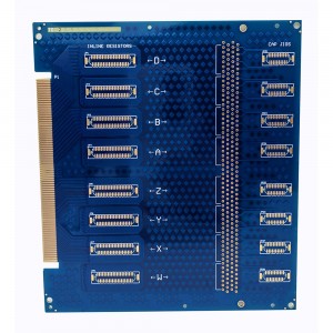
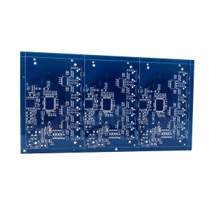
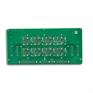
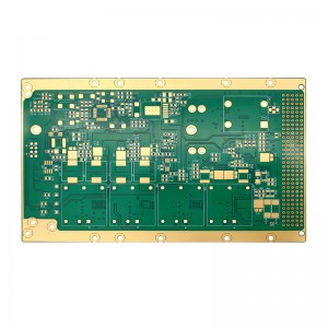
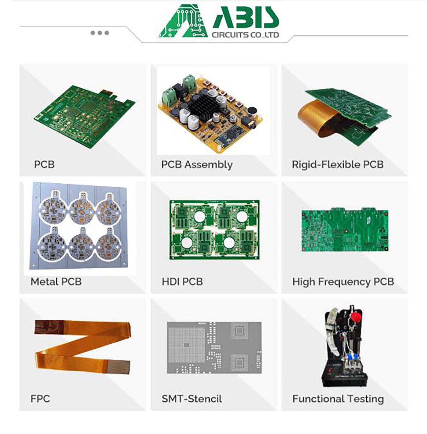
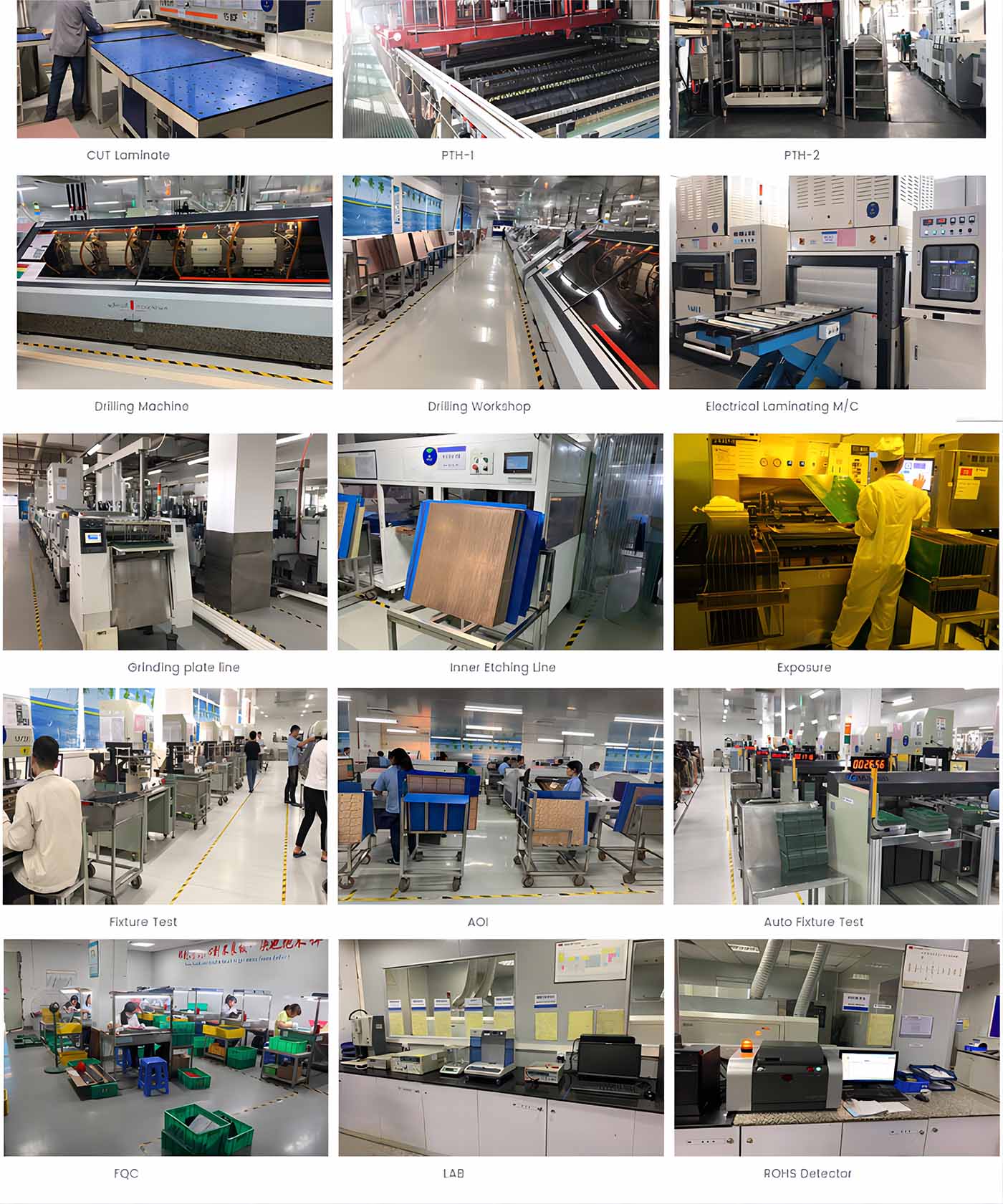
PCB Product&Equipment Show
Rigid PCB, Flexible PCB, Rigid-Flex PCB, HDI PCB, PCB Assembly
ABIS Quality Mission
Advanced equipment LIST
| AOI Testing | Checks for solder pasteChecks for components down to 0201
Checks for missing components, offset, incorrect parts, polarity |
| X-Ray Inspection | X-Ray provides high-resolution inspection of:BGAs/Micro BGAs/Chip scale packages /Bare boards |
| In-Circuit Testing | In-Circuit Testing is commonly used in conjunction with AOI minimizing functional defects caused by component problems. |
| Power-up Test | Advanced Function TestFlash Device Programming
Functional testing |
IOC incoming inspection
SPI solder paste inspection
Online AOI inspection
SMT first article inspection
External assessment
X-RAY-welding inspection
BGA device rework
QA inspection
Anti-static warehousing and shipment
Pursue 0% complaint on quality
All department implements according to ISO and the related dept has to provide 8D report if any board scrapped to defective.
All the outgoing boards have to be 100% electronic tested, impedance tested and soldering.
Visual inspected, we make the inspect microsection before shipment.
Train the mindset of employees and our enterprise culture, make they happy with their work and our company, it's helpful for them to produce good quality products.
High quality raw material (Shengyi FR4, ITEQ, Taiyo Solder Mask Ink etc.)
The AOI could inspect the whole set, boards are inspected after each process
Certificate


FAQ
To ensure an accurate quote, be sure to include the following information for your project:
Complete GERBER files including the BOM list
l Quantities
l Turn time
l Panelization Requirements
l Materials Requirements
l Finish requirements
l Your custom quote will be delivered in just 2-24 hours, depending on the design complexity.
Each Customer will have a sale to contact you. Our working hours: AM 9:00-PM 19:00(Beijing Time) from Monday to Friday. We will reply to your email as soon as quickly during our working time. And you also could contact our sales by cellphone if urgent.
ISO9001, ISO14001,UL USA& USA Canada,IFA16949, SGS, RoHS report.
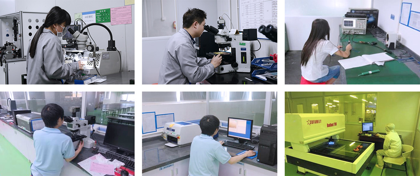
Our Quality Assuring Procedures as below:
a),Visual Inspection
b),Flying probe, fixture tool
c), Impedance control
d), Solder-ability detection
e), Digital metallo graghic microscope
f),AOI (Automated Optical Inspection)
Yes, we are pleased to supply module samples to test and check the quality, mixed sample order is available. Please note buyer should pay for the shipping cost.
On time delivery rate is more than 95%
a),24 hours fast turn for double side prototype PCB
b),48hours for 4-8 layers prototype PCB
c),1 hour for quotation
d),2 hours for engineer question/Complaint feedback
e),7-24 hours for technical support/order service/manufacturing operations
ABIS never choose orders. Both Small orders and Mass orders are welcome and We ABIS will be seriously and responsible, and serve customers with quality and quantity.
ABlS performs 100% visual and AOl inspection as well as performing electrical testing, high voltage testing, impedance control testing, micro-sectioning, thermal shock testing, solder testing, reliability testing, insulating resistance testing, ionic cleanliness testing and PCBA Functional testing.
a),1 Hour quotation
b),2 hours of complaint feedback
c),7*24 hour technical support
d),7*24 order service
e),7*24 hour delivery
f),7*24 production run
|
Production capacity of hot-sale products |
|
|
Double Side/Multilayer PCB Workshop |
Aluminum PCB Workshop |
|
Technical Capability |
Technical Capability |
|
Raw materials: CEM-1, CEM-3, FR-4(High TG), Rogers, TELFON |
Raw materials: Aluminum base, Copper base |
|
Layer: 1 layer to 20 Layers |
Layer: 1 layer and 2 Layers |
|
Min.line width/space: 3mil/3mil(0.075mm/0.075mm) |
Min.line width/space: 4mil/4mil(0.1mm/0.1mm) |
|
Min.Hole size: 0.1mm(dirilling hole) |
Min. Hole size: 12mil(0.3mm) |
|
Max. Board size: 1200mm* 600mm |
Max.Board size: 1200mm* 560mm(47in* 22in) |
|
Finished board thickness: 0.2mm- 6.0mm |
Finished board thickness: 0.3~ 5mm |
|
Copper foil thickness: 18um~280um(0.5oz~8oz) |
Copper foil thickness: 35um~210um(1oz~6oz) |
|
NPTH Hole Tolerance: +/-0.075mm, PTH hole Tolerance: +/-0.05mm |
Hole position tolerance: +/-0.05mm |
|
Outline Tolerance: +/-0.13mm |
Routing outline tolerance: +/ 0.15mm; punching outline tolerance:+/ 0.1mm |
|
Surface finished: Lead-free HASL, immersion gold(ENIG), immersion silver, OSP, gold plating, gold finger, Carbon INK. |
Surface finished: Lead free HASL, immersion gold(ENIG), immersion silver, OSP etc |
|
Impedance control tolerance: +/-10% |
Remain thickness tolerance: +/-0.1mm |
|
Production capability: 50,000 s.q.m/month |
MC PCB Production capability: 10,000 s.q.m/month |