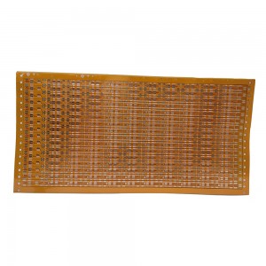
2 layers Custom PI Stiffeners Flexible Printed Circuit Boards PCBs


Basic Info
| Model No. | PCB-A42 |
| Transport package | Vacuum Packing |
| Certification | UL,ISO9001&ISO14001,RoHS |
| Application | Consumer electronics |
| Minimum Space/Line | 0.075mm/3mil |
| Production Capacity | 720, 000 M2/Year |
| HS Code | 853400900 |
| Origin | Made in China |
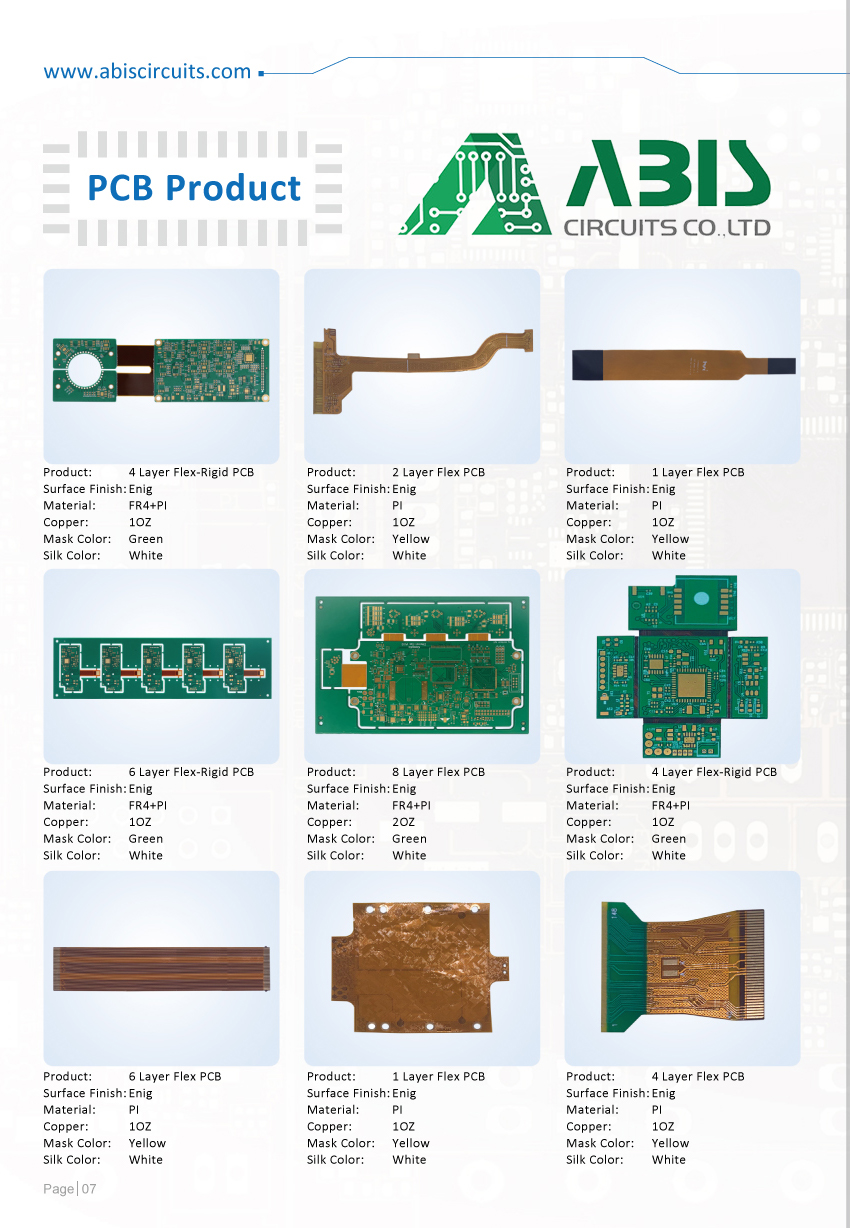
Product Description
Flexible printed circuit board overview
Definition
Flexible PCB – Flexible Printed Circuit, referred to as FPC.
A flexible printed circuit can be defined as an outline of conductive traces bonded on a flexible substrate. It is made into conductor circuit patterns using light pattern expose transfer and etching processes on the surface of a flexible substrate.
Characteristics
Flex circuits widely used in mobile phones, cameras and smart wearable.
It can better fit wiring capability in spaces than the traditional rigid boards.Flexible circuit boards also have better resistance to high temperatures, shock and vibrations. it has good performance with design challenges such as: unavoidable crossovers, specific impedance requirements, elimination of cross talk, additional shielding and high component density.
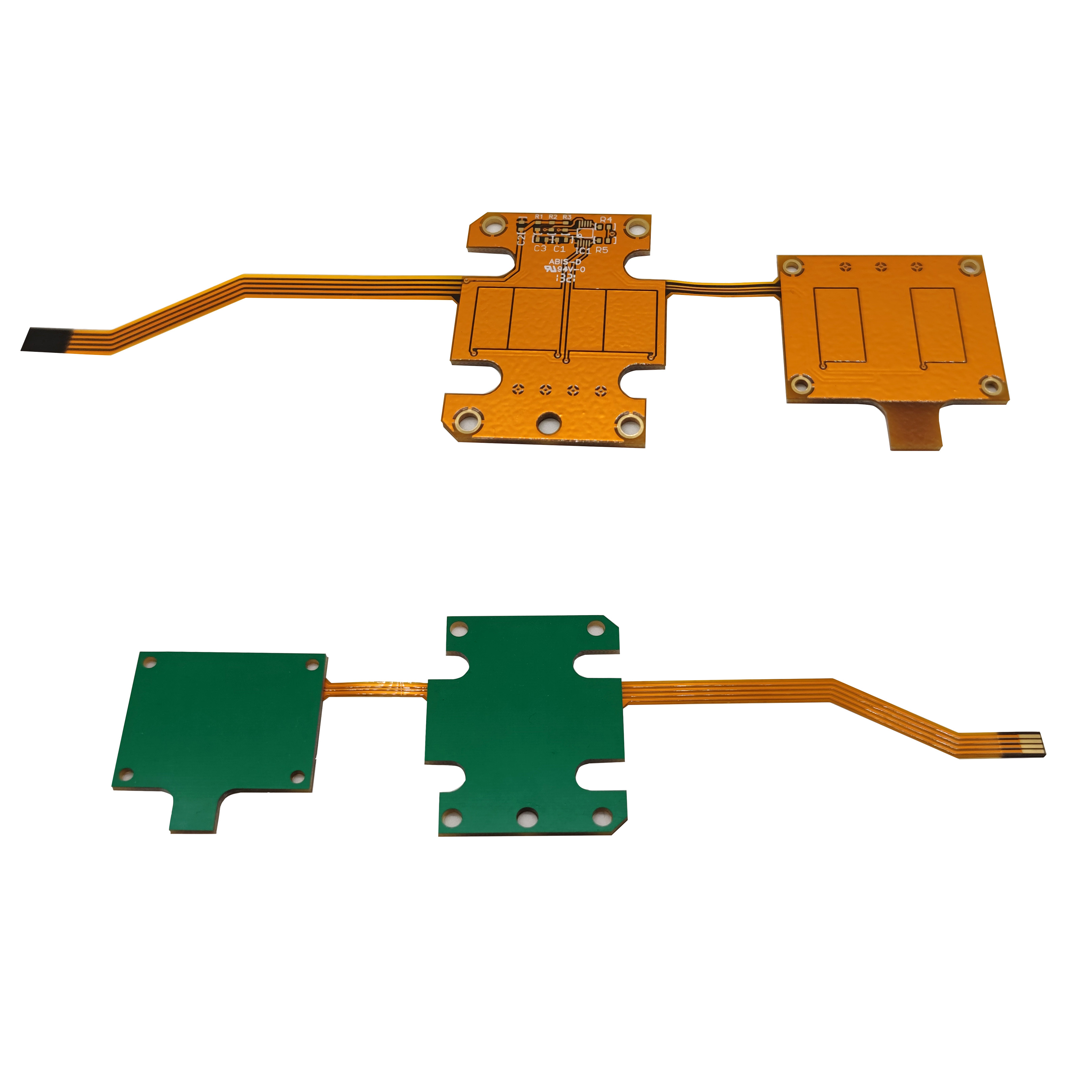
Classify
Single-sided flex PCB
Single-sided flex with dual access
Double-sided flex PCB
Multi-layer flex PCB
Technical & Capability
|
Item |
Speci. |
|
Layers |
1~8 |
|
Board Thickness |
0.1mm-0.2mm |
|
Substrate Material |
PI(0.5mil,1mil,2mil),PET(0.5mil,1mil) |
|
Conductive Medium |
Copper foil(1/3oz,1/2oz,1oz,2oz) Constantan Silver Paste Copper Ink |
|
Max Panel Size |
600mm×1200mm |
|
Min Hole Size |
0.1mm |
|
Min Line Width/Space |
3mil(0.075mm) |
|
Maximum imposition size (single & double panel) |
610mm*1200mm(Exposure limit) 250mm*35mm(only develop test samples) |
|
Maximum imposition size (single panel & double panel no PTH self-drying ink + UV light solid) |
610*1650mm |
|
Drilling Hole (Mechanical) |
17um--175um |
|
Finish Hole (Mechanical) |
0.10mm--6.30mm |
|
Diameter Tolerance (Mechanical) |
0.05mm |
|
Registration (Mechanical) |
0.075mm |
|
Aspect Ratio |
2:1(Minimum aperture 0.1mm) 5:1(Minimum aperture 0.2mm) 8:1(Minimum aperture 0.3mm) |
|
SMT Mini. Solder Mask Width |
0.075mm |
|
Mini. Solder Mask Clearance |
0.05mm |
|
Impedance Control Tolerance |
士10% |
|
Surface finish |
ENIG, HASL, Chem. Tin/Sn |
|
Solder mask/Protective Film |
PI(0.5mil,1mil,2mil)(Yellow, White, Black) PET(1mil,2mil) Solder mask (green, yellow, black...) |
|
Silkscreen |
Red/Yellow/Black/White |
|
Certificate |
UL, ISO 9001, ISO14001, IATF16949 |
|
Special Request |
Glue(3M467,3M468,3M9077,TESA8853...) |
|
Material Suppliers |
Shengyi, ITEQ, Taiyo, etc. |
|
Common Package |
Vacuum+Carton |
|
Monthly production capacity/m² |
60,000 m² |
Flexible PCB Lead Time
|
Small Batch Volume ≤1 sq meter |
Working Days |
Mass Production |
Working Days |
|
Single-Sided |
3-4 |
Single-Sided |
8-10 |
|
2-4 layers |
4-5 |
2-4 layers |
10-12 |
|
6-8 layers |
10-12 |
6-8 layers |
14-18 |
How ABIS Dealing With Flexible PCB Issues?
The first thing we ensure is the right equipment to produce your board. Next, the staff experienced enough to handle the challenge of manufacturing flexible boards.
Opening a solder mask or overlay enough-different steps of the process might change how a flexible board looks. Etching and plating can adjust the shape of the PCB, which is why you should ensure that overlay openings are of suitable width.
Choose the materials carefully, also considering other things, such as size, weight, and reliability of the board.
Control appropriate proximity of solder joints and bending point – the solder joint should be at the required distance from the bending location. If you put them too close, delamination or broken solder pad may occur.
Control Solder pad spacing – ABIS ensuring there is enough space between the pads and the conductive traces adjacent to them, so that avoiding lamination loss.
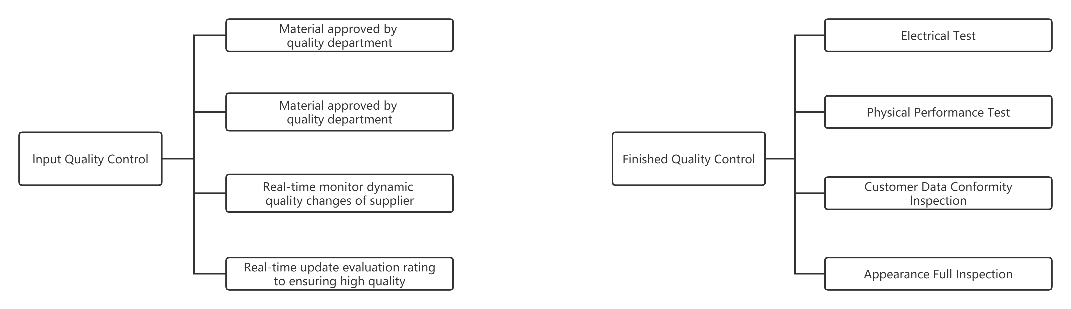
ABIS Quality Mission
The pass rate of incoming material above 99.9%, the number of mass rejection rates below 0.01%.
ABIS certified facilities control all key processes to eliminate all potential issues before producing.
ABIS utilizes advanced software to perform extensive DFM analysis on incoming data, and uses advanced quality control systems throughout the manufacturing process.
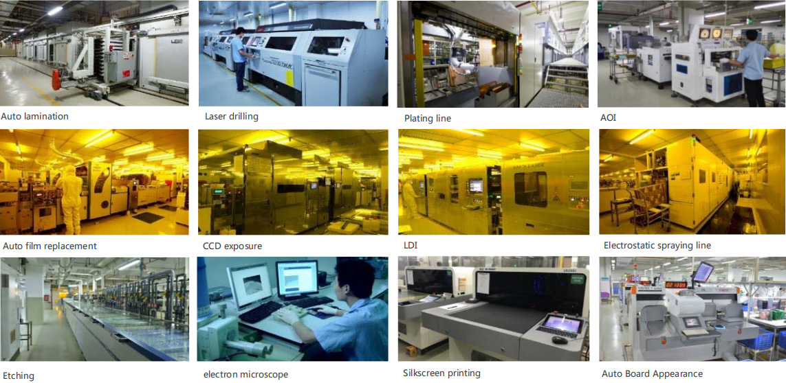
ABIS performs 100% visual and AOI inspection as well as performing electrical testing, high voltage testing, impedance control testing, micro-sectioning, thermal shock testing, solder testing, reliability testing, insulating resistance testing and ionic cleanliness testing.
Certificate


FAQ
Each Customer will have a sale to contact you. Our working hours: AM 9:00-PM 19:00(Beijing Time) from Monday to Friday. We will reply to your email as soon as quickly during our working time. And you also could contact our sales by cellphone if urgent.
Our Quality Assuring Procedures as below:
a),Visual Inspection
b),Flying probe, fixture tool
c), Impedance control
d), Solder-ability detection
e), Digital metallograghic microscope
f),AOI (Automated Optical Inspection)
Generally 2-3 days for sample making. The lead time of mass production will depend on the order quantity and the season you place the order.
Our Quality Assuring Procedures as below:
a),Visual Inspection
b),Flying probe, fixture tool
c), Impedance control
d), Solder-ability detection
e), Digital metallograghic microscope
f),AOI (Automated Optical Inspection)
ABIS has no MOQ requirements for either PCB or PCBA.
ABlS performs 100% visual and AOl inspection as well as performing electrical testing, high voltage testing, impedance control testing, micro-sectioning, thermal shock testing, solder testing, reliability testing, insulating resistance testing, ionic cleanliness testing and PCBA Functional testing.
Please send the details inquiry to us, such as the Item Number, Quantity for each item, Quality request, Logo, Payment Terms, Transport method, Discharge place, etc. We will make an accurate quotation for you as soon as possible.
On time delivery rate is more than 95%
a),24 hours fast turn for double side prototype PCB
b),48hours for 4-8 layers prototype PCB
c),1 hour for quotation
d),2 hours for engineer question/Complaint feedback
e),7-24 hours for technical support/order service/manufacturing operations
| Production capacity of hot-sale products | |
| Double Side/Multilayer PCB Workshop | Aluminum PCB Workshop |
| Technical Capability | Technical Capability |
| Raw materials: CEM-1, CEM-3, FR-4(High TG), Rogers, TELFON | Raw materials: Aluminum base, Copper base |
| Layer: 1 layer to 20 Layers | Layer: 1 layer and 2 Layers |
| Min.line width/space: 3mil/3mil(0.075mm/0.075mm) | Min.line width/space: 4mil/4mil(0.1mm/0.1mm) |
| Min.Hole size: 0.1mm(dirilling hole) | Min. Hole size: 12mil(0.3mm) |
| Max. Board size: 1200mm* 600mm | Max.Board size: 1200mm* 560mm(47in* 22in) |
| Finished board thickness: 0.2mm- 6.0mm | Finished board thickness: 0.3~ 5mm |
| Copper foil thickness: 18um~280um(0.5oz~8oz) | Copper foil thickness: 35um~210um(1oz~6oz) |
| NPTH Hole Tolerance: +/-0.075mm, PTH hole Tolerance: +/-0.05mm | Hole position tolerance: +/-0.05mm |
| Outline Tolerance: +/-0.13mm | Routing outline tolerance: +/ 0.15mm; punching outline tolerance:+/ 0.1mm |
| Surface finished: Lead-free HASL, immersion gold(ENIG), immersion silver, OSP, gold plating, gold finger, Carbon INK. | Surface finished: Lead free HASL, immersion gold(ENIG), immersion silver, OSP etc |
| Impedance control tolerance: +/-10% | Remain thickness tolerance: +/-0.1mm |
| Production capability: 50,000 s.q.m/month | MC PCB Production capability: 10,000 s.q.m/month |