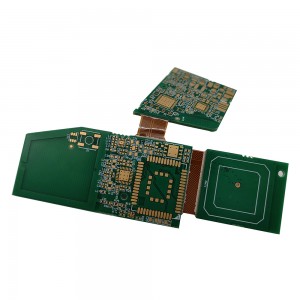
Customizable 6 Layers Rigid-Flex PCB Board with 3.0oz Copper and ENIG 2u” Surface Finish

Basic Info
| Model No. | PCB-A35 |
| Transport package | Vacuum Packing |
| Certification | UL,ISO9001&ISO14001,RoHS |
| Definitions | IPC Class2 |
| Minimum Space/Line | 0.075mm/3mil |
| Impedance control | 50±10% |
| Production Capacity | 720, 000 M2/Year |
| Origin | Made in China |
Product Description
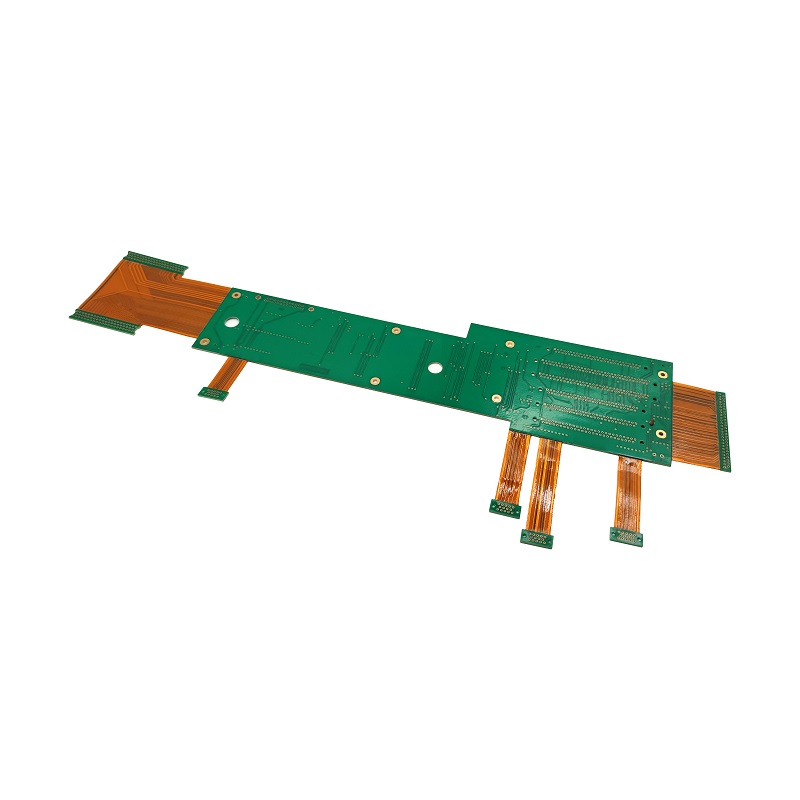
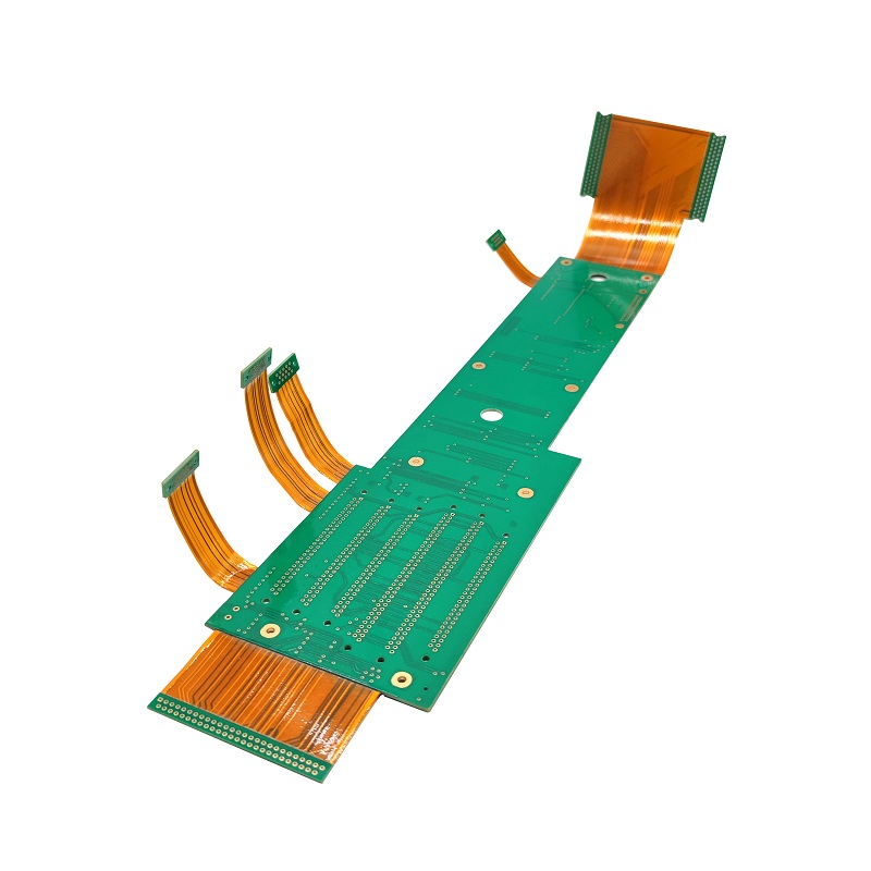
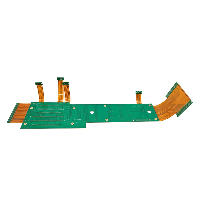
Rigid-flexible printed circuits boards overview
The literal meaning of "rigid-flex" is combination the advantages of both flexible and rigid boards. It's seen as two-in-one circuit is interconnected through plated thru holes. Rigid flex circuits enable higher component density while fitting into limited and odd shaped spaces.
Rigid-flex printed circuits boards consists of multiple flexible circuit inner layers selectively attached together using an epoxy pre-preg bonding film, similar to a multilayer flexible circuit. Rigid flex circuits have been used in the military and aerospace industries for more than 20 years. In most rigid flex circuit boards.
Technical & Capability
| Item | Production Capacity |
| Layer Counts | 1-32 |
| Material | FR-4, High TG FR-4, PTFE, Aluminum Base, Cu base, Rogers, Teflon, etc |
| Maximum Size | 600mm X1200mm |
| Board Outline Tolerance | ±0.13mm |
| Board Thickness | 0.20mm--8.00mm |
| Thickness Tolerance(t≥0.8mm) | ±10% |
| Thickness Tolerancc(t<0.8mm) | ±0.1mm |
| Insulation Layer Thickncss | 0.075mm--5.00mm |
| Minimum Iine | 0.075mm |
| Minimum Space | 0.075mm |
| Out Layer Copper Thickness | 18um--350um |
| Inner Layer Copper Thickness | 17um--175um |
| Drilling Hole(Mechanical) | 0.15mm--6.35mm |
| Finish Hole(Mechanical) | 0.10mm--6.30mm |
| Diameter Tolerance(Mechanical) | 0.05mm |
| Registration(Mechanical) | 0.075mm |
| Aspecl Ratio | 16:01 |
| Solder Mask Type | LPI |
| SMT Mini.Solder Mask Width | 0.075mm |
| Mini.Solder Mask Clearance | 0.05mm |
| Plug Hole Diameter | 0.25mm--0.60mm |
| Impedance Control Tolerance | 10% |
| Surface Finish | HASL/HASL-LF, ENIG, Immersion Tin/Silver, Flash Gold, OSP ,Gold finger, Hard Gold |
Manufacturing Capability-(Flex)
| items | unit | ||||||
| Max layers | Layer | 10 | |||||
| Base Material (Polymide) | μm | 9, 12, 18, 35, 70 | |||||
| Copper foil | μm | 18,35,70 | |||||
| Coverlayer (Polymide) | μm | 27.5, 37.5, 50, 75 | |||||
| Thermosetting Cement | μm | 13, 25 | |||||
| Maximal Panel Size | mm | 250*800 | 250*1500 for 10 Layers | ||||
| Minimum Panel Size | mm | Depends on the customer | |||||
| Maximal Finished Board Thickness | mm | 0.7 | |||||
| Minimum Finished Board Thickness | mm | 0.057mm | |||||
| Hole size Tolerance | mm | ±0.05mm | |||||
| Minimum Through Hole | mm | 0.1mm | |||||
| Minimum Through Hole Pad | mm | 0.3mm | 0.25mm Particular | ||||
| Maximal Base Copper Thickness | OZ | 2 | |||||
| Minimum Base Copper Thickness | OZ | 1/4 | |||||
| Copper Plating Thickness | μm | 8-20 | |||||
| PTH Copper Thickness | μm | 8~20 | |||||
| Minimum Line Width/Spacing | mm | 0.05 | |||||
| Surface Finished | / | Ni,Au,Sn | |||||
Flexible PCB Lead Time
|
Small Batch Volume ≤1 sq meter |
Working Days |
Mass Production |
Working Days |
|
Single-Sided |
3-4 |
Single-Sided |
8-10 |
|
2-4 layers |
4-5 |
2-4 layers |
10-12 |
|
6-8 layers |
10-12 |
6-8 layers |
14-18 |
Advantages of ABIS
- High-end equipment-high speed Pick and Place Machines that can process about 25,000 SMD components per hour
- High efficient supply ability 60K Sqm monthly-Offers low volume and on-demand PCB production, also large-scale production
- Professional engineering team-40 engineers and their own tooling house, strong at OEM. Offers two easy options: Custom and Standard-In-depth knowledge of IPC Class II and III Standards
We provide a comprehensive turn-key EMS service to customers who want us to assemble the PCB into PCBA, including prototypes, NPI projects, small and medium volumes. We are also able to source all components for your PCB assembly project. Our engineers and sourcing team have rich experience in the supply chain and EMS industry, with deep knowledge in SMT assembly allowing us to resolve all the production issues. Our service is cost-effective, flexible, and reliable. We have satisfied customers across many industries including medical, industrial, automotive, and consumer electronics.
Certificate


FAQ
ABIS's Main Industries: Industrial Control, Telecommunication, Automotive Products and Medical. ABIS's Main Market: 90% International Market(40%-50% for USA, 35% for Europe, 5% for Russia and 5%-10% for East Asia) and 10% Domestic Market.
Main Suppliers(FR4): Kingboard (Hong Kong), NanYa (Taiwan), and Shengyi (China), If others, please RFQ.
Our Quality Assuring Procedures as below:
a),Visual Inspection
b),Flying probe, fixture tool
c), Impedance control
d), Solder-ability detection
e), Digital metallograghic microscope
f),AOI (Automated Optical Inspection)
Generally 2-3 days for sample making. The lead time of mass production will depend on the order quantity and the season you place the order.
Our Quality Assuring Procedures as below:
a),Visual Inspection
b),Flying probe, fixture tool
c), Impedance control
d), Solder-ability detection
e), Digital metallograghic microscope
f),AOI (Automated Optical Inspection)
ABlS performs 100% visual and AOl inspection as well as performing electrical testing, high voltage testing, impedancecontrol testing, micro-sectioning, thermal shock testing, solder testing, reliability testing, insulating resistance testing, ionic cleanliness testing and PCBA Functional testing.
ABlS performs 100% visual and AOl inspection as well as performing electrical testing, high voltage testing, impedance control testing, micro-sectioning, thermal shock testing, solder testing, reliability testing, insulating resistance testing, ionic cleanliness testing and PCBA Functional testing.
ABIS has no MOQ requirements for either PCB or PCBA.
On time delivery rate is more than 95%
a),24 hours fast turn for double side prototype PCB
b),48hours for 4-8 layers prototype PCB
c),1 hour for quotation
d),2 hours for engineer question/Complaint feedback
e),7-24 hours for technical support/order service/manufacturing operations