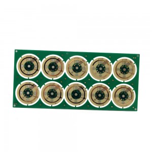
FR4 TG150 PCB Board Double-sided Circuits borad with Hard gold 3u” and Counter sink/bore


Basic Info
| Model No. | PCB-A34 |
| Transport package | Vacuum Packing |
| Certification | UL,ISO9001&ISO14001,RoHS |
| Application | Consumer electronics |
| Minimum Space/Line | 0.075mm/3mil |
| Production Capacity | 50,000 s.q.m/month |
| HS Code | 853400900 |
| Origin | Made in China |
Product Description
FR4 PCB Introduction
FR means “flame-retardant,” FR-4 (or FR4) is a NEMA grade designation for glass-reinforced epoxy laminate material, a composite material composed of woven fiberglass cloth with an epoxy resin binder that makes it an ideal substrate for electronic components on a printed circuit board.
Pros and Cons of FR4 PCB
FR-4 material is so popular because of its many wondrous qualities that can benefit printed circuit boards. In addition to being affordable and easy to work with, it is an electrical insulator with very high dielectric strength. Plus, it's durable, moisture-resistant, temperature-resistant and lightweight.
FR-4 is a widely relevant material, popular mostly for its low cost and relative mechanical and electrical stability. While this material features extensive benefits and is available in a variety of thicknesses and sizes, it isn't the best choice for every application, especially high-frequency applications like RF and microwave designs.
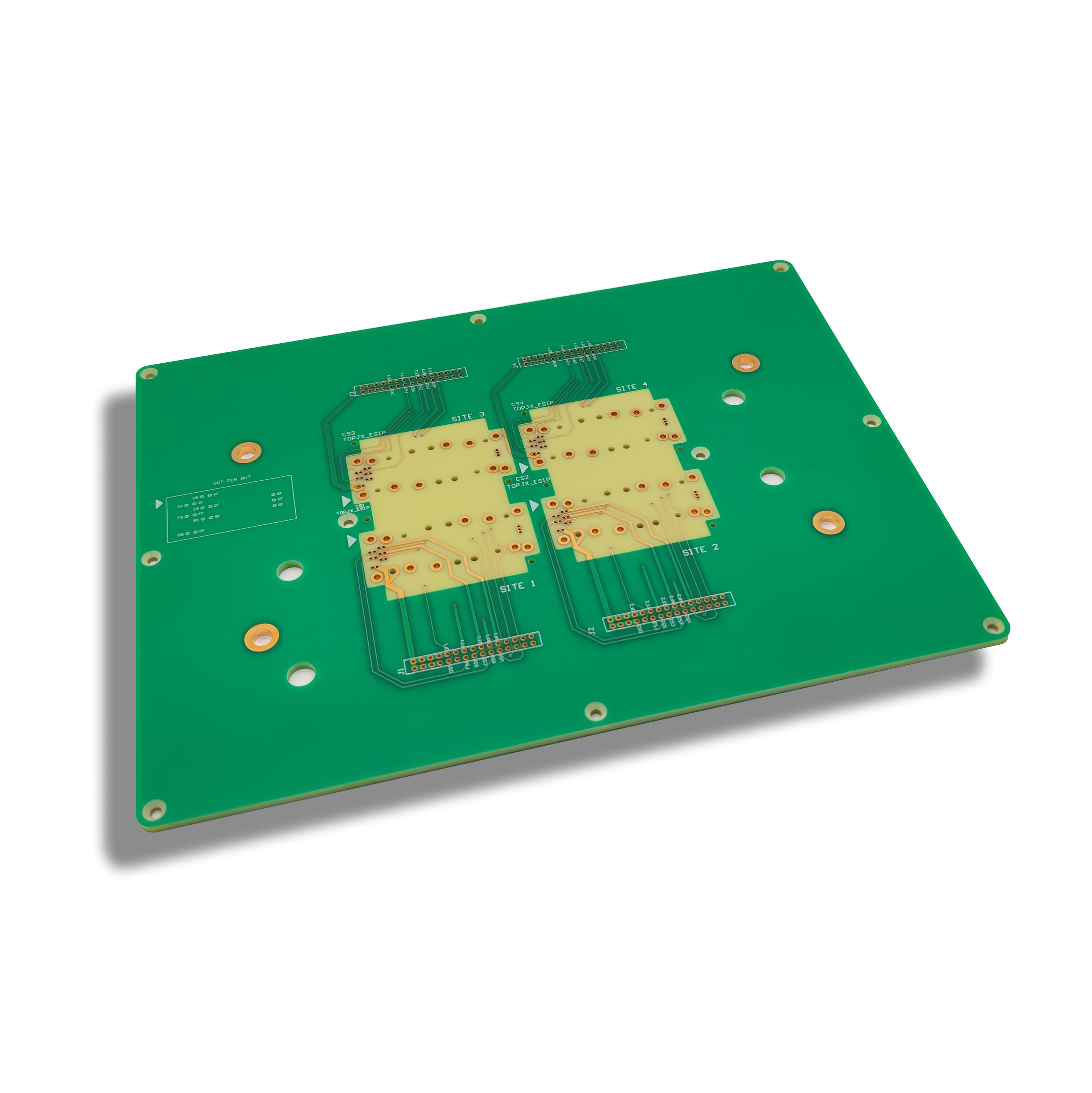
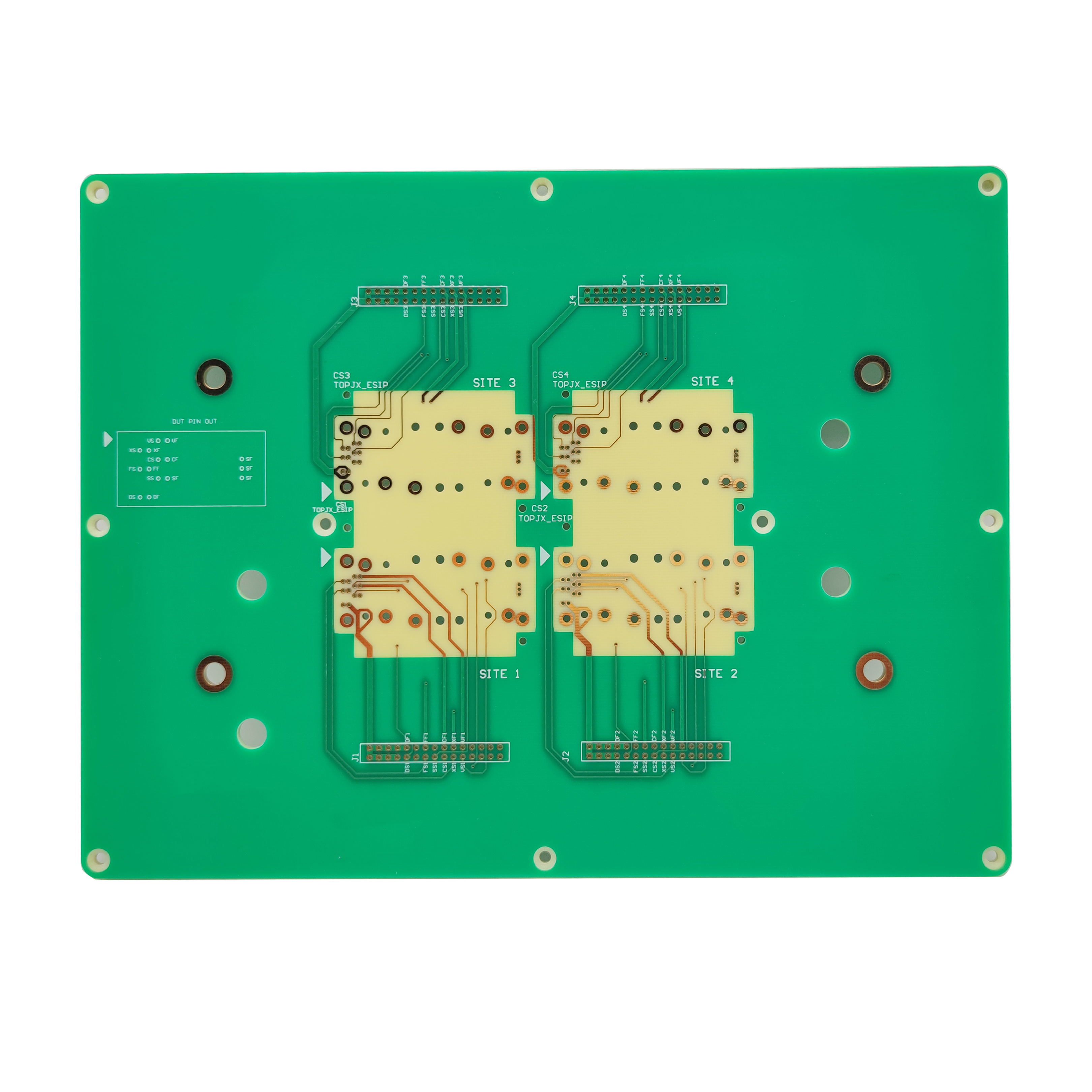
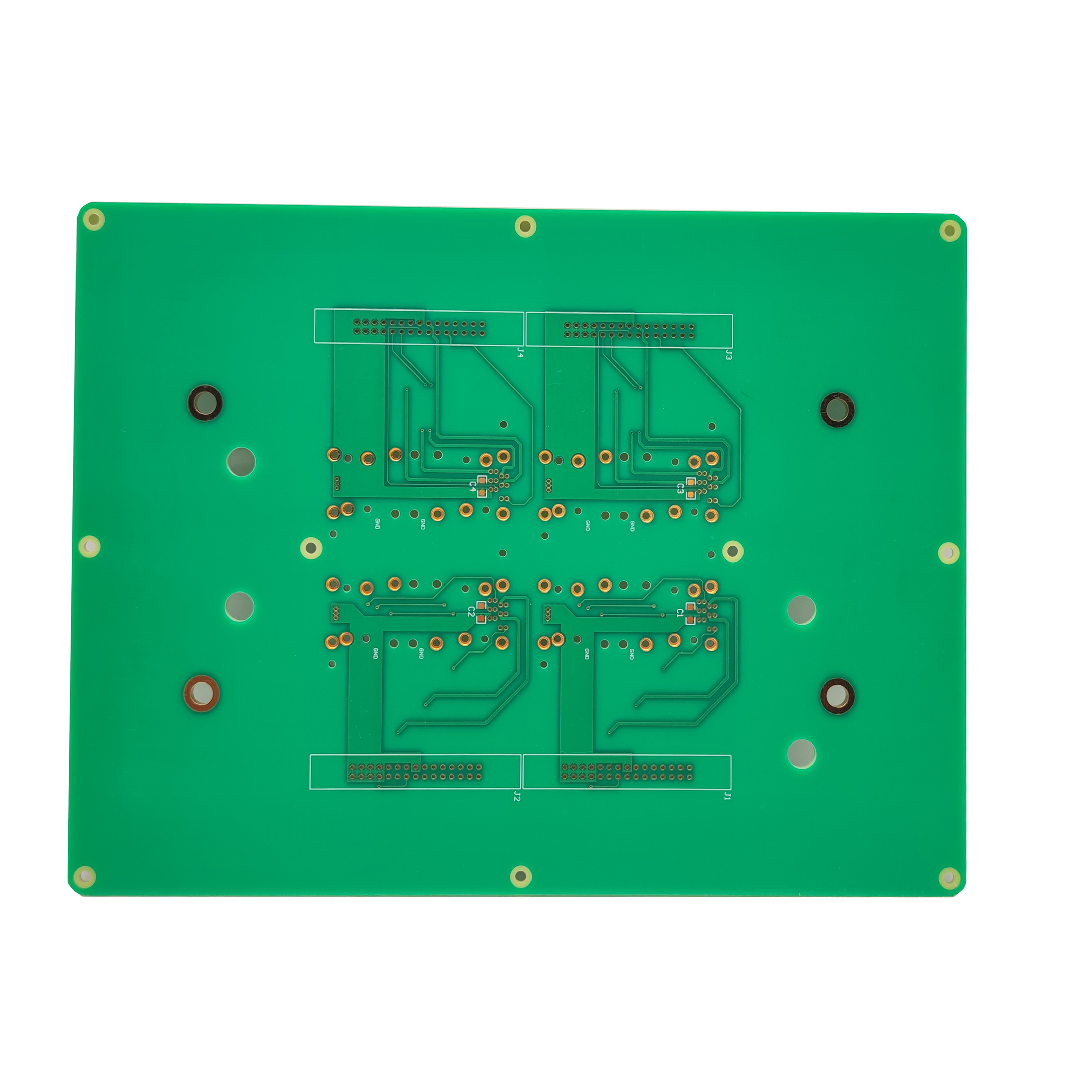
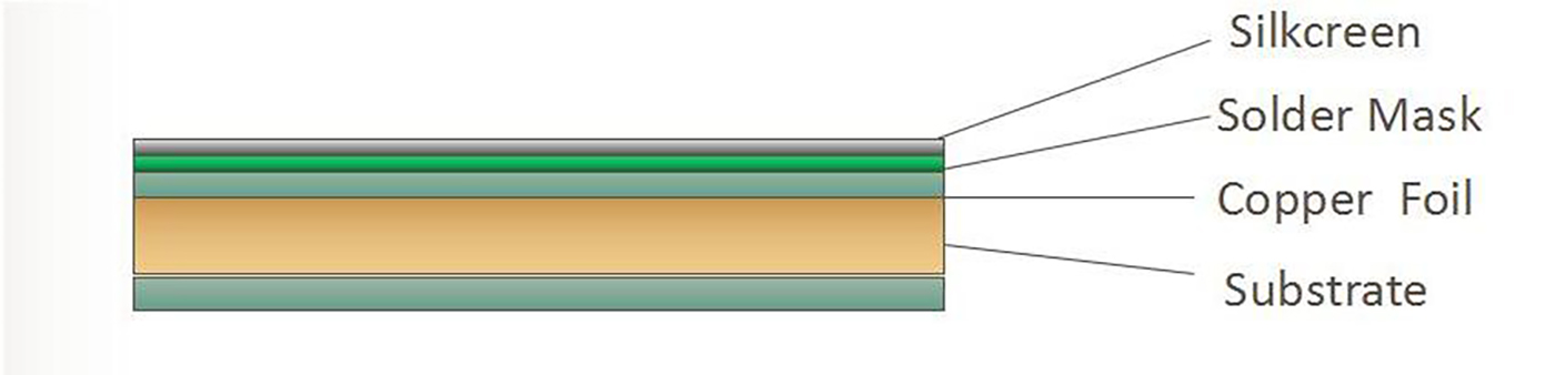
Multi-layer PCB Structure
Multilayer PCBs further increases the complexity and density of PCB designs by adding additional layers beyond the top and bottom layers seen in double sided boards. Multilayer PCBs are built by laminating the various layers. The inner-layers, normally double-sided circuit boards, are stacked together, with insulating layers in between and between the copper-foil for the outer-layers. Holes drilled through the board (vias) will make connections with the different layers of the board.
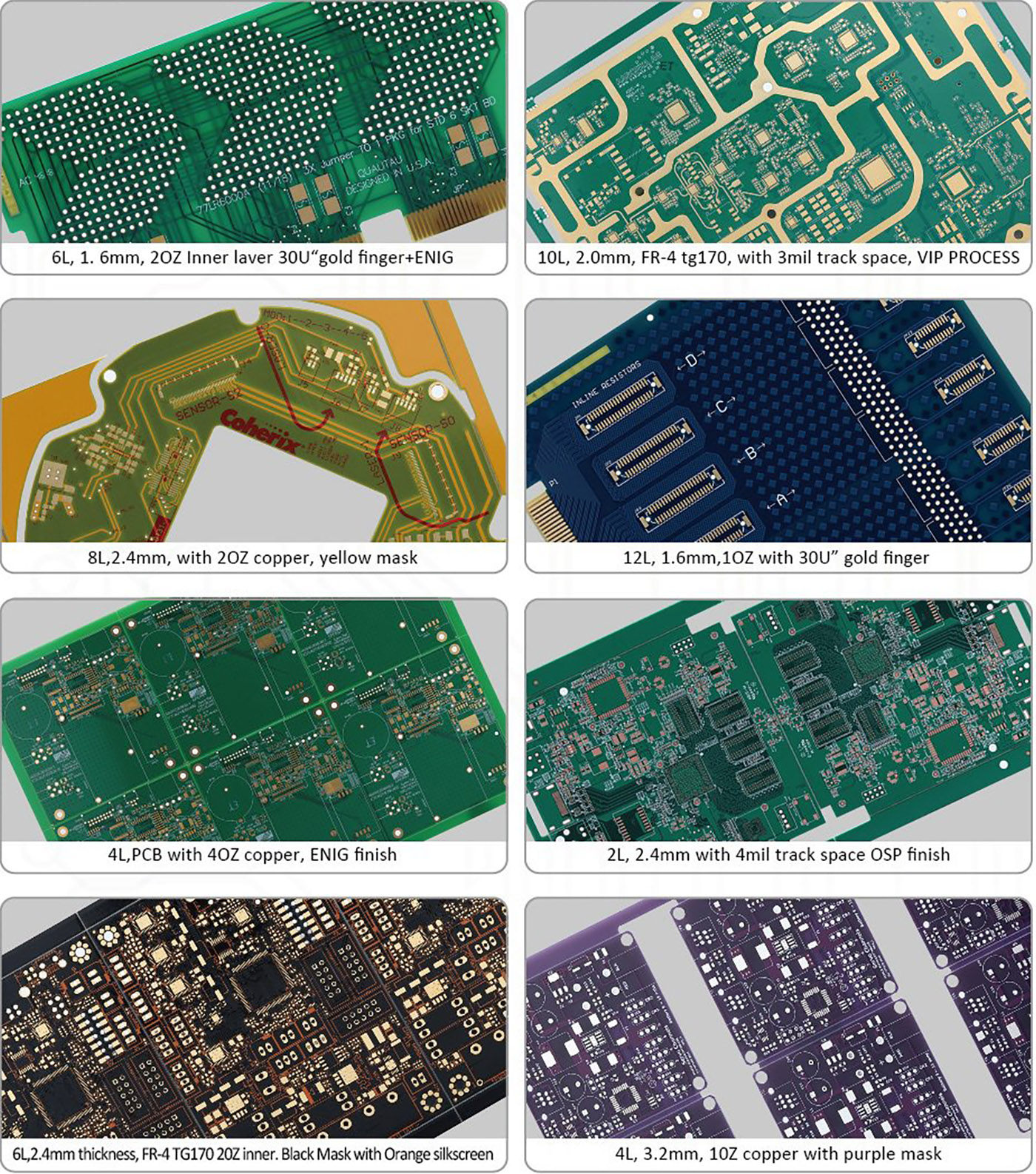
Technical & Capability
| ITEM | CAPABILITY | ITEM | CAPABILITY |
| Layers | 1-20L | Thicker Copper | 1-6OZ |
| Products Type | HF(High-frequency) &(Radio Frequency)board, Imedance controlled board, HDIboard, BGA & Fine Pitch board | Solder Mask | Nanya & Taiyo; LRI & Matt Red. green,yellow, white, blue, black |
| Base material | FR4(Shengyi China,ITEQ, KB A+,HZ),HITG,FrO6,Rogers,Taconic,Argon,Nalco lsola and so on | Finished Surface | Conventional HASL,Lead-free HASL,FlashGold,ENIG (lmmersion Gold) OSP (Entek),lmmersion TiN, lmmersion Silver,Hard Gold |
| Selective Surface treatment | ENIG(immersion Gold) + OSP ,ENIG(immersion Gold) + Gold Finger, Flash Gold Finger, immersionSlive + Gold Finger, Immersion Tin + Gold Finger | ||
| Technical Specification | Minimum line width/gap: 3.5/4mil (laser dril) Minimum hole size: 0.15 mm(mechanical drill/4 mill laser drill) Minimum Annular Ring: 4mil Max Copper thickness: 6Oz Max Production size: 600x1200mm Board Thickness: D/S: 0.2-70mm,Mulltilayers: 0.40-7.Omm Min Solder Mask Bridge: ≥0.08mm Aspect ratio: 15:1 Plugging vias capability: 0.2-0.8mm |
||
| Tolerance | Plated holes Tolerance : ±0.08mm(min±0.05) Non-plated hole tolerance: ±O.05min(min+O/-005mm or +0.05/Omm) Outline Tolerance: ±0.15min(min±0.10mm) Functional test: lnsulating resistance: 50 ohms (normality) Peel off strength: 14N/mm Thermal Stress test: 265C.20 seconds Solder mask hardness: 6H E-test voltage: 50ov±15/-0V 3os Warp and Twist: 0.7%( semiconductor test board 0.3%) |
||
Where does the resin material come from in ABIS?
Most of them from Shengyi Technology Co., Ltd. (SYTECH), who has been the world's second largest CCL manufacturer in terms of sales volume, from 2013 to 2017. We established long-term relations of cooperation since 2006. The FR4 resin material (Model S1000-2, S1141, S1165, S1600) are mainly used for making single and double-sided printed circuit boards as well as multi-layer boards. Here comes details for your reference.
For FR-4: Sheng Yi, King Board, Nan Ya, Polycard, ITEQ, ISOLA
For CEM-1 & CEM 3: Sheng Yi, King Board
For High Frequency : Sheng Yi
For UV Cure: Tamura, Chang Xing ( * Available colour : Green) Solder for Single Side
For Liquid Photo: Tao Yang, Resist (Wet Film)
Chuan Yu ( * Available colors : White, Imaginable Solder Yellow, Purple, Red, Blue, Green, Black)
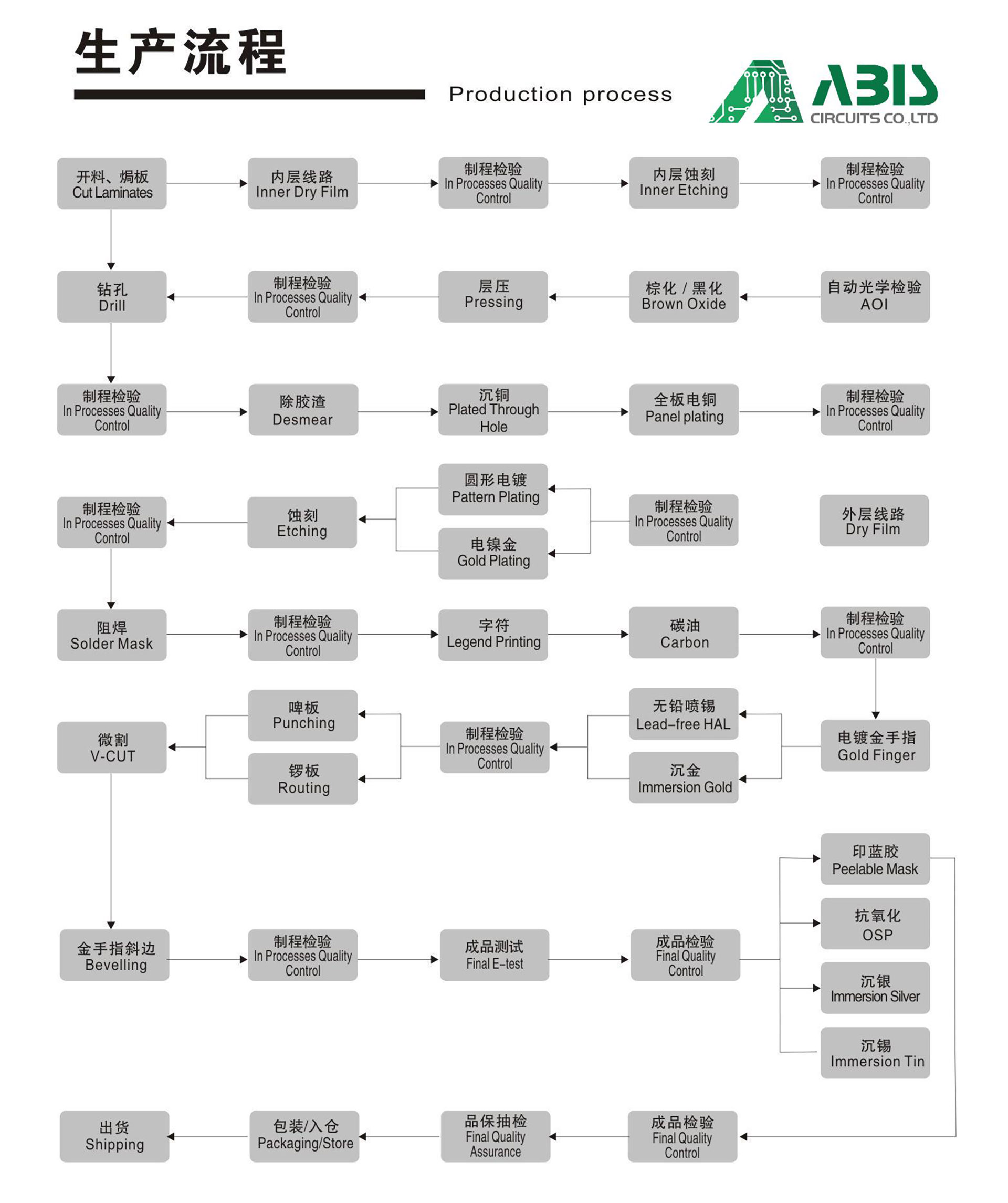
PCB Production Process
The process starts with designing Layout of the PCB using any PCB designing software / CAD Tool (Proteus, Eagle, Or CAD).
All rest of the steps are of Manufacturing Process of a Rigid Printed Circuit Board is same as Single Sided PCB or Double Sided PCB or Multi-layer PCB.
Q/T Lead Time
| Category | Quickest Lead Time | Normal Lead Time |
| Double-sided | 24hrs | 120hrs |
| 4 Layers | 48hrs | 172hrs |
| 6 Layers | 72hrs | 192hrs |
| 8 Layers | 96hrs | 212hrs |
| 10 Layers | 120hrs | 268hrs |
| 12 Layers | 120hrs | 280hrs |
| 14 Layers | 144hrs | 292hrs |
| 16-20 Layers | Depends on the specific requirements | |
| Above 20 Layers | Depends on the specific requirements | |
ABIS' move to control FR4 PCBS
Hole Preparation
Removing debris carefully & adjusting drill machine parameters: before plating through with copper, ABIS pays high attention to all holes on an FR4 PCB treated to remove debris, surface irregularities, and epoxy smear, the clean holes ensure the plating successfully adheres to the hole walls. also, early in the process, drill machine parameters are adjusted accurately.
Surface Preparation
Deburring carefully: our experienced tech workers will be aware ahead of time that the only way to avoid a bad outcome is to anticipate the need for special handling and to take the appropriate steps to be sure that the process is done carefully and correctly.
Thermal Expansion Rates
Accustomed to dealing with the various materials, ABIS will be able to analyze the combination to be sure that it is appropriate. then keeping the long-term reliability of the CTE (coefficient of thermal expansion), with the lower CTE, the less likely the plated through holes are to fail from repeated flexing of the copper which forms the internal layer interconnections.
Scaling
ABIS control the circuitry is scaled-up by known percentages in anticipation of this loss so that the layers will return to their as-designed dimensions after the lamination cycle is complete. also, using the laminate manufacturer’s baseline scaling recommendations in combination with in-house statistical process control data, to dial-in scale factors that will be consistent over time within that particular manufacturing environment.
Machining
When the time comes to build your PCB, ABIS be sure that you choose has the right equipment and experience to produce it correctly on the first try.
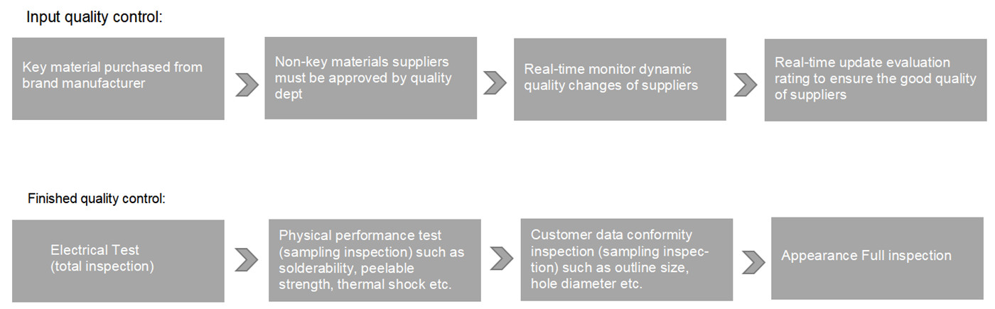
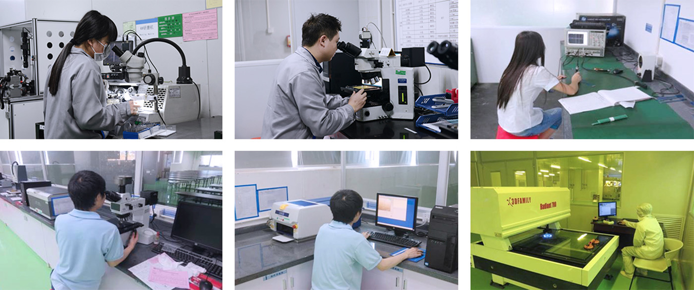
ABIS Quality Mission
The pass rate of incoming material above 99.9%, the number of mass rejection rates below 0.01%.
ABIS certified facilities control all key processes to eliminate all potential issues before producing.
ABIS utilizes advanced software to perform extensive DFM analysis on incoming data, and uses advanced quality control systems throughout the manufacturing process.
ABIS performs 100% visual and AOI inspection as well as performing electrical testing, high voltage testing, impedance control testing, micro-sectioning, thermal shock testing, solder testing, reliability testing, insulating resistance testing and ionic cleanliness testing.
Certificate


Why Chose us?
- High-end euipment-high speed Pick and Place Machines that can process about 25,000 SMD components per hour
- High efficient supply ability 60K Sqm monthly-Offers low volume and on-demand PCB production, also large-scale production
- Professional engineering team-40 engineers and their own tooling house, strong at OEM. Offers two easy options: Custom and Standard-In-depth knowledge of IPC Class II and III Standards
We provide a comprehensive turn-key EMS service to customers who want us to assemble the PCB into PCBA, including prototypes, NPI project, small and medium volume. We are also able to source all components for your PCB assembly project. Our engineers and sourcing team have rich experience in supply chain and EMS industry, with deep knowledges in SMT assembly allowing to resolve all the production issues. Our service is cost-effective, flexible, and reliable. We have satisfied customers across many industries including medical, industrial, automotive and consumer electronics.
FAQ
To ensure an accurate quote, be sure to include the following information for your project:
Complete GERBER files including the BOM list
l Quantities
l Turn time
l Panelization Requirements
l Materials Requirements
l Finish requirements
l Your custom quote will be delivered in just 2-24 hours, depending on the design complexity.
Checked within 12 hours. Once Engineer's question and working file checked, we'll start the production.
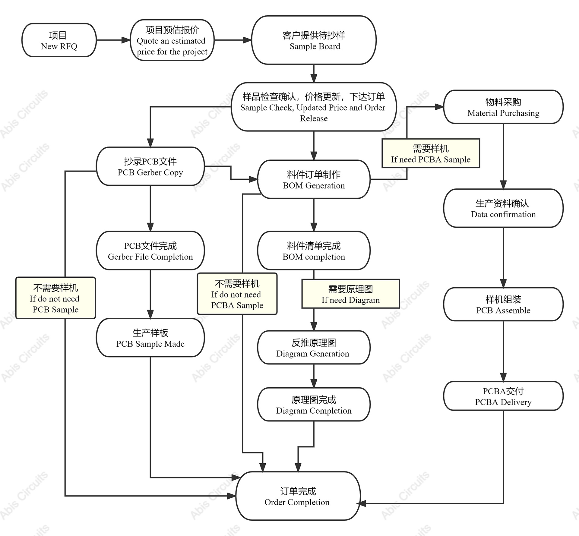
No, we can't accpet picture files, if you no not have gerber file, can you send us sample to copy it.
PCB&PCBA Copy Process:
Our Quality Assuring Procedures as below:
a),Visual Inspection
b),Flying probe, fixture tool
c), Impedance control
d), Solder-ability detection
e), Digital metallo graghic microscope
f),AOI (Automated Optical Inspection)
Yes, we are pleased to supply module samples to test and check the quality, mixed sample order is available. Please note buyer should pay for the shipping cost.
On time delivery rate is more than 95%
a),24 hours fast turn for double side prototype PCB
b),48hours for 4-8 layers prototype PCB
c),1 hour for quotation
d),2 hours for engineer question/Complaint feedback
e),7-24 hours for technical support/order service/manufacturing operations
ABlS performs 100% visual and AOl inspection as well as performing electrical testing, high voltage testing, impedancecontrol testing, micro-sectioning, thermal shock testing, solder testing, reliability testing, insulating resistance testing, ionic cleanliness testing and PCBA Functional testing.
| Production capacity of hot-sale products | |
| Double Side/Multilayer PCB Workshop | Aluminum PCB Workshop |
| Technical Capability | Technical Capability |
| Raw materials: CEM-1, CEM-3, FR-4(High TG), Rogers, TELFON | Raw materials: Aluminum base, Copper base |
| Layer: 1 layer to 20 Layers | Layer: 1 layer and 2 Layers |
| Min.line width/space: 3mil/3mil(0.075mm/0.075mm) | Min.line width/space: 4mil/4mil(0.1mm/0.1mm) |
| Min.Hole size: 0.1mm(dirilling hole) | Min. Hole size: 12mil(0.3mm) |
| Max. Board size: 1200mm* 600mm | Max.Board size: 1200mm* 560mm(47in* 22in) |
| Finished board thickness: 0.2mm- 6.0mm | Finished board thickness: 0.3~ 5mm |
| Copper foil thickness: 18um~280um(0.5oz~8oz) | Copper foil thickness: 35um~210um(1oz~6oz) |
| NPTH Hole Tolerance: +/-0.075mm, PTH hole Tolerance: +/-0.05mm | Hole position tolerance: +/-0.05mm |
| Outline Tolerance: +/-0.13mm | Routing outline tolerance: +/ 0.15mm; punching outline tolerance:+/ 0.1mm |
| Surface finished: Lead-free HASL, immersion gold(ENIG), immersion silver, OSP, gold plating, gold finger, Carbon INK. | Surface finished: Lead free HASL, immersion gold(ENIG), immersion silver, OSP etc |
| Impedance control tolerance: +/-10% | Remain thickness tolerance: +/-0.1mm |
| Production capability: 50,000 s.q.m/month | MC PCB Production capability: 10,000 s.q.m/month |
a),1 Hour quotation
b),2 hours of complaint feedback
c),7*24 hour technical support
d),7*24 order service
e),7*24 hour delivery
f),7*24 production run
a),1 Hour quotation
b),2 hours of complaint feedback
c),7*24 hour technical support
d),7*24 order service
e),7*24 hour delivery
f),7*24 production run