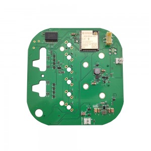
High-quality 2-Layer Customized PCBAs Specialized for Connectors


Basic Info
| Model No. | PCBA-A48 |
| Assembly method | Post Welding |
| Transport package | Anti-static Packaging |
| Certification | UL, ISO9001&14001, SGS, RoHS, Ts16949 |
| Definitions | IPC Class2 |
| Minimum Space/Line | 0.075mm/3mil |
| Application | Signal transmission |
| Origin | Made in China |
| Production Capacity | 720,000 M2/Year |
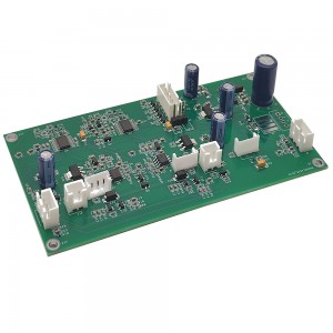
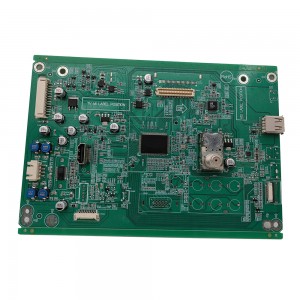
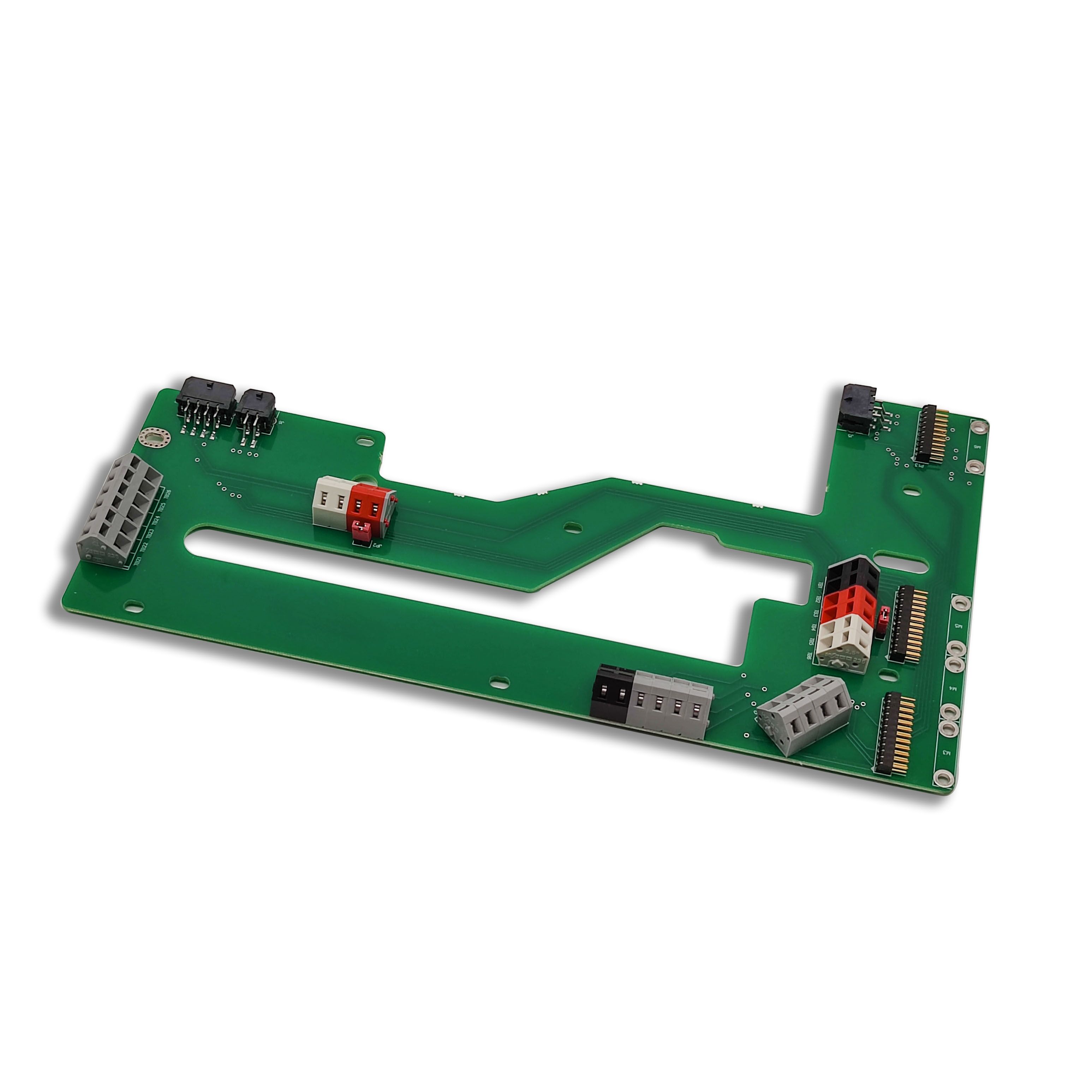
Product Description

PCBA Capabilities
| 1 | SMT assembly including BGA assembly |
| 2 | Accepted SMD chips: 0204, BGA, QFP, QFN, TSOP |
| 3 | Component height: 0.2-25mm |
| 4 | Min packing: 0201 |
| 5 | Min distance among BGA : 0.25-2.0mm |
| 6 | Min BGA size: 0.1-0.63mm |
| 7 | Min QFP space: 0.35mm |
| 8 | Min assembly size: (X*Y): 50*30mm |
| 9 | Max assembly size: (X*Y): 350*550mm |
| 10 | Pick-placement precision: ±0.01mm |
| 11 | Placement capability: 0805, 0603, 0402 |
| 12 | High pin count press fit available |
| 13 | SMT capacity per day: 80,000 points |
Capability - SMT
|
Lines |
9(5 Yamaha,4KME) |
|
Capacity |
52 million placements per month |
|
Max Board Size |
457*356mm.(18”X14”) |
|
Min Component size |
0201-54 sq.mm.(0.084 sq.inch),long connector,CSP,BGA,QFP |
|
Speed |
0.15 sec/chip,0.7 sec/QFP |
Capability - PTH
|
Lines |
2 |
|
Max board width |
400 mm |
|
Type |
Dual wave |
|
Pbs status |
Lead-free line support |
|
Max temp |
399 degree C |
|
Spray flux |
add-on |
|
Pre-heat |
3 |
Q/T Lead Time
| Category | Quickest Lead Time | Normal Lead Time |
| Double-sided | 24hrs | 120hrs |
| 4 Layers | 48hrs | 172hrs |
| 6 Layers | 72hrs | 192hrs |
| 8 Layers | 96hrs | 212hrs |
| 10 Layers | 120hrs | 268hrs |
| 12 Layers | 120hrs | 280hrs |
| 14 Layers | 144hrs | 292hrs |
| 16-20 Layers | Depends on the specific requirements | |
| Above 20 Layers | Depends on the specific requirements | |
Quality Control
| AOI Testing | Checks for solder pasteChecks for components down to 0201
Checks for missing components, offset, incorrect parts, polarity |
| X-Ray Inspection | X-Ray provides high-resolution inspection of:BGAs/Micro BGAs/Chip scale packages /Bare boards |
| In-Circuit Testing | In-Circuit Testing is commonly used in conjunction with AOI minimizing functional defects caused by component problems. |
| Power-up Test | Advanced Function TestFlash Device Programming
Functional testing |
- IOC incoming inspection
- SPI solder paste inspection
- Online AOI inspection
- SMT first article inspection
- External assessment
- X-RAY-welding inspection
- BGA device rework
- QA inspection
- Anti-static warehousing and shipment
FAQ
A:
Bill of materials (BOM) detailing:
a), Manufacturers parts numbers,
b), Components suppliers' parts number (e.g. Digi-key, Mouser, RS )
c), PCBA sample photos if possible.
d), Quantity
A: Free samples depend on your order quantity.
A:
No, we can't accpet picture files, if you no not have gerber file, can you send us sample to copy it.
PCB&PCBA Copy Process:

A:
Our Quality Assuring Procedures as below:
a),Visual Inspection
b),Flying probe, fixture tool
c), Impedance control
d), Solder-ability detection
e), Digital metallograghic microscope
f),AOI (Automated Optical Inspection)
A: Please send the details inquiry to us, such as the Item Number, Quantity for each item, Quality request, Logo, Payment Terms, Transport method, Discharge place, etc. We will make an accurate quotation for you as soon as possible.
A: Each Customer will have a sale to contact with you. Our working hours: AM 9:00-PM 19:00(Beijing Time) from Monday to Friday. We will reply to your email as soon as quickly during our working time. And you also could contact our sales by cellphone if urgent.
A: Yes, we are pleased to supply module samples to test and check the quality, mixed sample order is available. Please note buyer should pay for the shipping cost.
A: yes, We have a professional drawing engineers' team that you can trust.
A: Yes, we ensure that each piece of PCB, and PCBA will be tested before shipment, and we ensure the goods we sent with good quality.
A: We suggest you use DHL, UPS, FedEx, and TNT forwarder.
A: By T/T, Paypal, Western Union, etc.