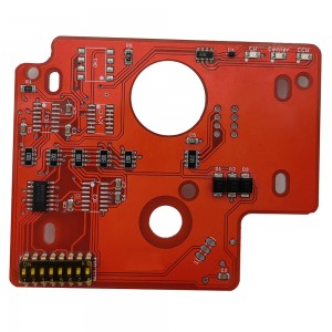
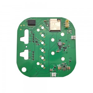
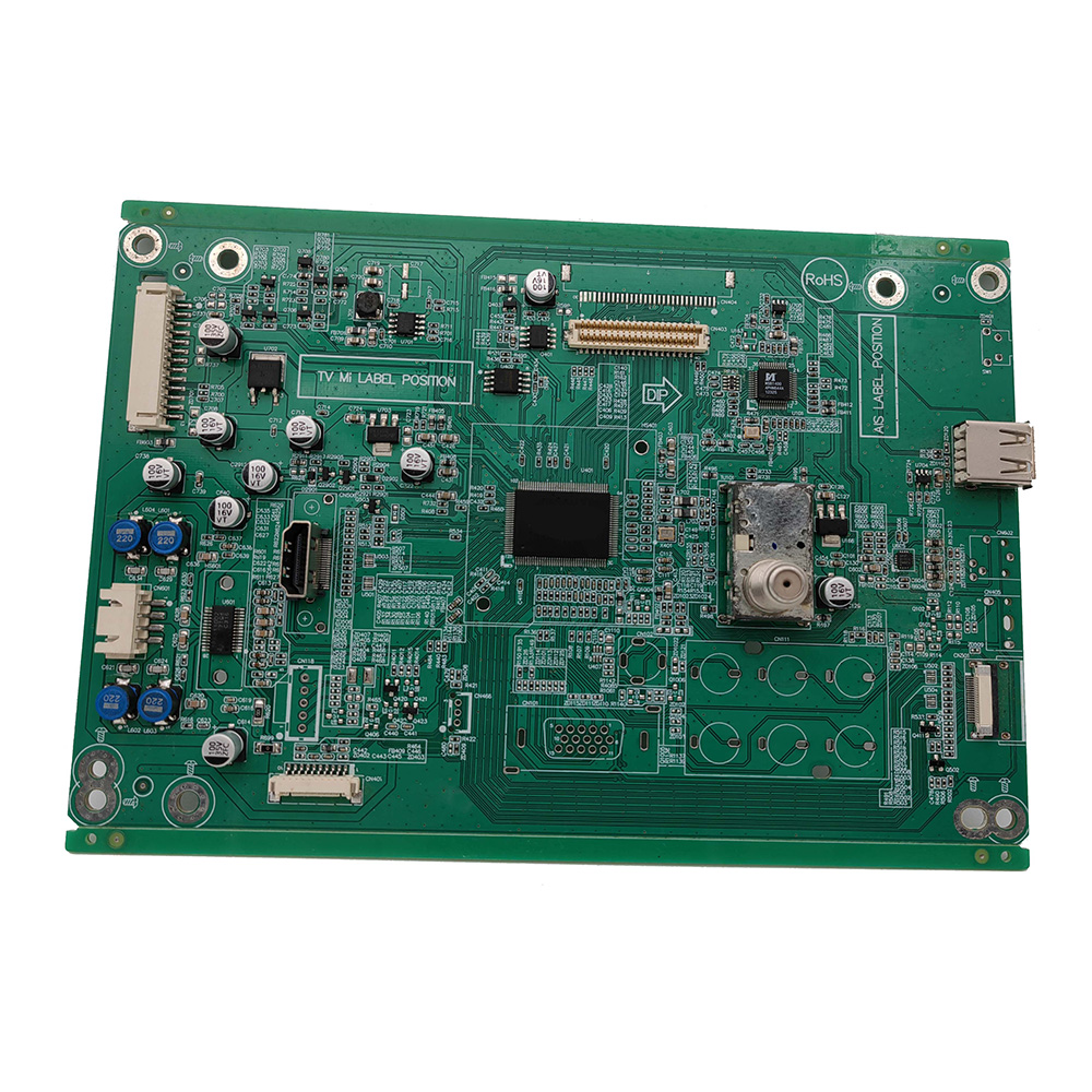
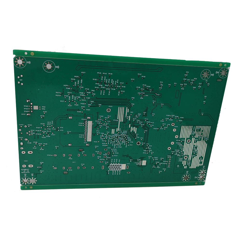
Turn-key 4 layers PCB Assembly Board High quality FR4 Multilayer PCBA
Manufacturing info
| Model No. | PCB-A3 |
| Transport package | Vacuum Packing |
| Certification | UL,ISO9001&ISO14001,RoHS |
| Definitions | IPC Class2 |
| Minimum Space/Line | 0.075mm/3mil |
| Origin | Made in China |
| Production Capacity | 720,000 M2/Year |
| Application | Consumer Electronics |
Product Description
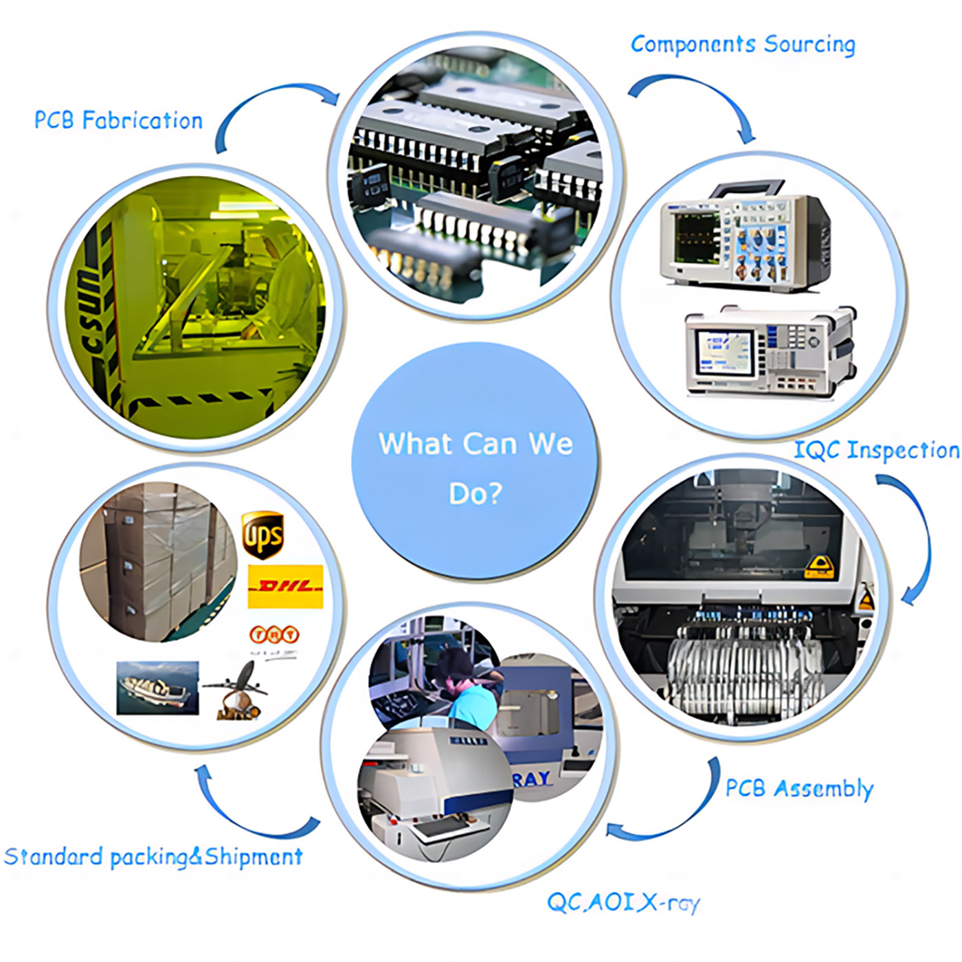
PCBA Projects Introduction
ABIS CIRCUITS Company deliver services, not only products. We offer solutions, not only goods.
From the PCB production, the components purchasing to the components assemble. Includes:
PCB Custom
PCB drawing / design according to your schematic diagram
PCB manufacturing
Component sourcing
PCB Assemble
PCBA 100% test
Our Advantages
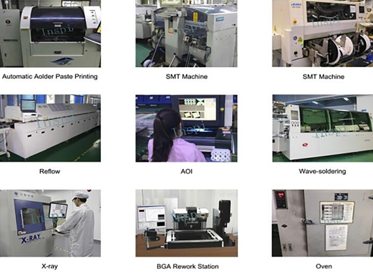
High-end equipment-high speed Pick and Place Machines that can process about 25,000 SMD components per hour
High efficient supply ability 60K Sqm monthly-Offers low volume and on-demand PCB production, also large-scale productions
Professional engineering team-40 engineers and their own tooling house, strong at OEM. Offers two easy options: Custom and Standard-In-depth knowledge of IPC Class II and III Standards
We provide a comprehensive turn-key EMS service to customers who want us to assemble the PCB into PCBA, including prototypes, NPI project, small and medium volume. We are also able to source all components for your PCB assembly project. Our engineers and sourcing team have rich experience in supply chain and EMS industry, with deep knowledges in SMT assembly allowing to resolve all the production issues. Our service is cost-effective, flexible, and reliable. We have satisfied customers across many industries including medical, industrial, automotive and consumer electronics.
PCBA Capabilities
|
Capacity |
|
|
Single and double-sided SMT/PTH |
Yes |
|
Large parts on both sides, BGA on both sides |
Yes |
|
Smallest Chips size |
0201 |
|
Min BGA and Micro BGA pitch and ball counts |
0.008 in. (0.2mm) pitch, ball count greater than 1000 |
|
Min Leaded parts pitch |
0.008 in. (0.2 mm) |
|
Max Parts size assembly by machine |
2.2 in. x 2.2 in. x 0.6 in. |
|
Assembly surface mount connectors |
Yes |
|
Odd form parts: |
Yes, Assembly by hands |
|
LED |
|
|
Resistor and capacitor networks |
|
|
Electrolytic capacitors |
|
|
Variable resistors and capacitors (pots) |
|
|
Sockets |
|
|
Reflow soldering |
Yes |
|
Max PCB size |
14.5 in. x 19.5 in. |
|
Min PCB Thickness |
0.2 |
|
Fiducial Marks |
Preferred but not required |
|
PCB Finish: |
1.SMOBC/HASL |
|
2.Electrolytic gold |
|
|
3.Electroless gold |
|
|
4.Electroless silver |
|
|
5.Immersion gold |
|
|
6.Immersion tin |
|
|
7.OSP |
|
|
PCB Shape |
Any |
|
Panelized PCB |
1.Tab routed |
|
2.Breakaway tabs |
|
|
3.V-Scored |
|
|
4.Routed+ V scored |
|
|
Inspection |
1.X-ray analysis |
|
2.Microscope to 20X |
|
|
Rework |
1.BGA removal and replacement station |
|
2.SMT IR rework station |
|
|
3.Thru-hole rework station |
|
|
Firmware |
Provide programming firmware files,Firmware + software installation instructions |
|
Function test |
Level of testing required along with test instructions |
|
PCB file: |
PCB Altium/Gerber/Eagle files (Including specs such as thickness, copper thickness, solder mask colour, finish, etc) |
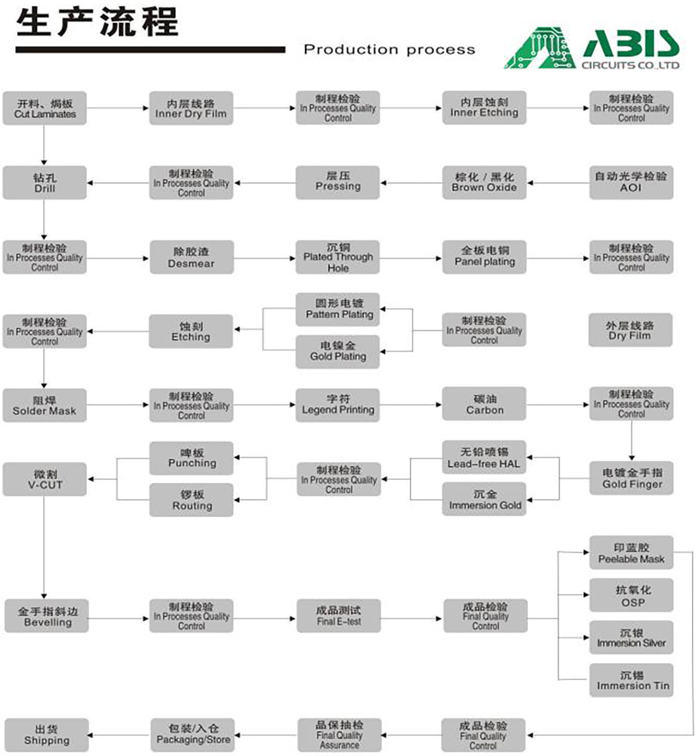
Production Processes
Material Receiving → IQC → Stock → Material to SMT → SMT Line Loading → Solder Paste/Glue Printing → Chip Mount → Reflow → 100% Visual Inspection → Automated Optical Inspection (AOI) → SMT QC Sampling → SMT Stock → Material to PTH → PTH Line Loading → Plated Through Hole → Wave Soldering → Touch Up → 100% Visual Inspection → PTH QC Sampling → In-Circuit Test (ICT) → Final Assembly → Functional Test (FCT) → Packing → OQC Sampling → Shipping
Quality Control
| AOI Testing | Checks for solder paste
Checks for components down to 0201 Checks for missing components, offset, incorrect parts, polarity |
| X-Ray Inspection | X-Ray provides high-resolution inspection of:
BGAs/Micro BGAs/Chip scale packages /Bare boards |
| In-Circuit Testing | In-Circuit Testing is commonly used in conjunction with AOI minimizing functional defects caused by component problems. |
| Power-up Test | Advanced Function Test
Flash Device Programming Functional testing |
IOC incoming inspection
SPI solder paste inspection
Online AOI inspection
SMT first article inspection
External assessment
X-RAY-welding inspection
BGA device rework
QA inspection
Anti-static warehousing and shipment
Certificate


FAQ
Each Customer will have a sale to contact you. Our working hours: AM 9:00-PM 19:00(Beijing Time) from Monday to Friday. We will reply to your email as soon as quickly during our working time. And you also could contact our sales by cellphone if urgent.
Bill of materials (BOM) detailing:
a), Manufacturers parts numbers,
b), Components suppliers' parts number (e.g. Digi-key, Mouser, RS )
c), PCBA sample photos if possible.
d), Quantity
ISO9001, ISO14001,UL USA& USA Canada,IFA16949, SGS, RoHS report.
No, we can't accept picture files, if you no not have Gerber file, can you send us sample to copy it.
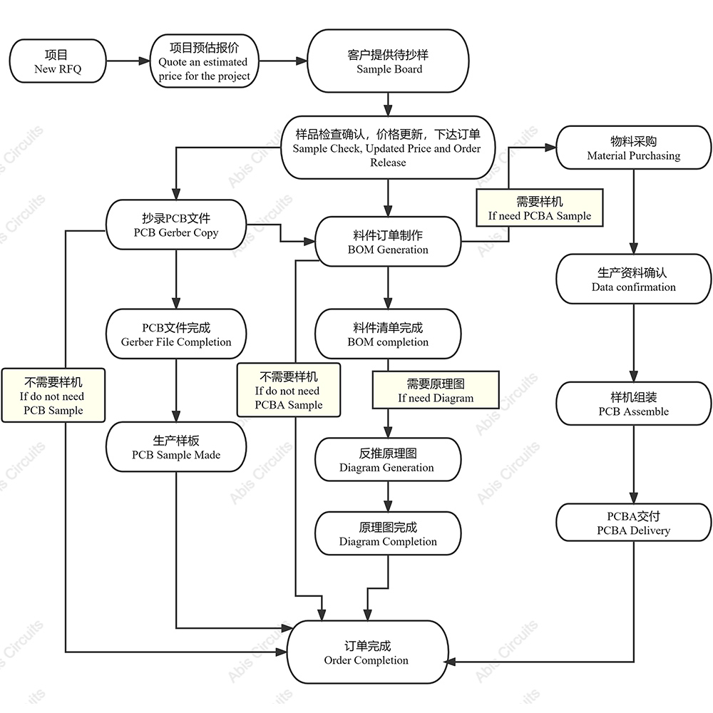
PCB&PCBA Copy Process:
Our Quality Assuring Procedures as below:
a),Visual Inspection
b),Flying probe, fixture tool
c), Impedance control
d), Solder-ability detection
e), Digital metallograghic microscope
f),AOI (Automated Optical Inspection)
ABlS performs 100% visual and AOl inspection as well as performing electrical testing, high voltage testing, impedance control testing, micro-sectioning, thermal shock testing, solder testing, reliability testing, insulating resistance testing, ionic cleanliness testing and PCBA Functional testing.
ABIS has a dedicated team responsible for after-sales service. If there is any problem after the product is sold, you can feedback to the sales. We will reply you and deal with it as soon as we receive your contact.
ABIS is very confident in our PCB and PCBA boards, all the material and components are the best and original, the customer complaint rate is very low.
On time delivery rate is more than 95%
a),24 hours fast turn for double side prototype PCB
b),48hours for 4-8 layers prototype PCB
c),1 hour for quotation
d),2 hours for engineer question/Complaint feedback
e),7-24 hours for technical support/order service/manufacturing operations