China Customize PCB&PCBA Design and Manufacturing PCB Assembly Circuit Board


Manufacturing info
| Model No. | PCB-A45 |
| Assembly method | SMT |
| Transport package | Anti-static Packaging |
| Certification | UL, ISO9001&14001, SGS, RoHS, Ts16949 |
| Definitions | IPC Class2 |
| Minimum Space/Line | 0.075mm/3mil |
| Application | Communication |
| Origin | Made in China |
| Production Capacity | 720,000 M2/Year |
Product Description
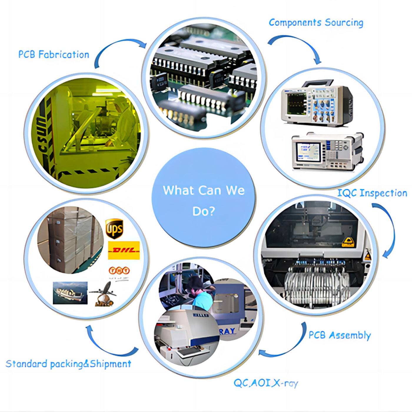
PCBA Projects Introduction
ABIS CIRCUITS Company deliver services, not only products. We offer solutions, not only goods.
From the PCB production, the components purchasing to the components assemble. Includes:
PCB Custom
PCB drawing / design according to your schematic diagram
PCB manufacturing
Component sourcing
PCB Assemble
PCBA 100% test
Production Processes
Material Receiving → IQC → Stock → Material to SMT → SMT Line Loading → Solder Paste/Glue Printing → Chip Mount → Reflow → 100% Visual Inspection → Automated Optical Inspection (AOI) → SMT QC Sampling → SMT Stock → Material to PTH → PTH Line Loading → Plated Through Hole → Wave Soldering → Touch Up → 100% Visual Inspection → PTH QC Sampling → In-Circuit Test (ICT) → Final Assembly → Functional Test (FCT) → Packing → OQC Sampling → Shipping
PCBA Capabilities
| 1 | SMT assembly including BGA assembly |
| 2 | Accepted SMD chips: 0204, BGA, QFP, QFN, TSOP |
| 3 | Component height: 0.2-25mm |
| 4 | Min packing: 0204 |
| 5 | Min distance among BGA : 0.25-2.0mm |
| 6 | Min BGA size: 0.1-0.63mm |
| 7 | Min QFP space: 0.35mm |
| 8 | Min assembly size: (X*Y): 50*30mm |
| 9 | Max assembly size: (X*Y): 350*550mm |
| 10 | Pick-placement precision: ±0.01mm |
| 11 | Placement capability: 0805, 0603, 0402 |
| 12 | High pin count press fit available |
| 13 | SMT capacity per day: 80,000 points |
Capability - SMT
|
Lines |
9(5 Yamaha,4KME) |
|
Capacity |
52 million placements per month |
|
Max Board Size |
457*356mm.(18”X14”) |
|
Min Component size |
0201-54 sq.mm.(0.084 sq.inch),long connector,CSP,BGA,QFP |
|
Speed |
0.15 sec/chip,0.7 sec/QFP |
Capability - PTH
|
Lines |
2 |
|
Max board width |
400 mm |
|
Type |
Dual wave |
|
Pbs status |
Lead-free line support |
|
Max temp |
399 degree C |
|
Spray flux |
add-on |
|
Pre-heat |
3 |
Quality Control
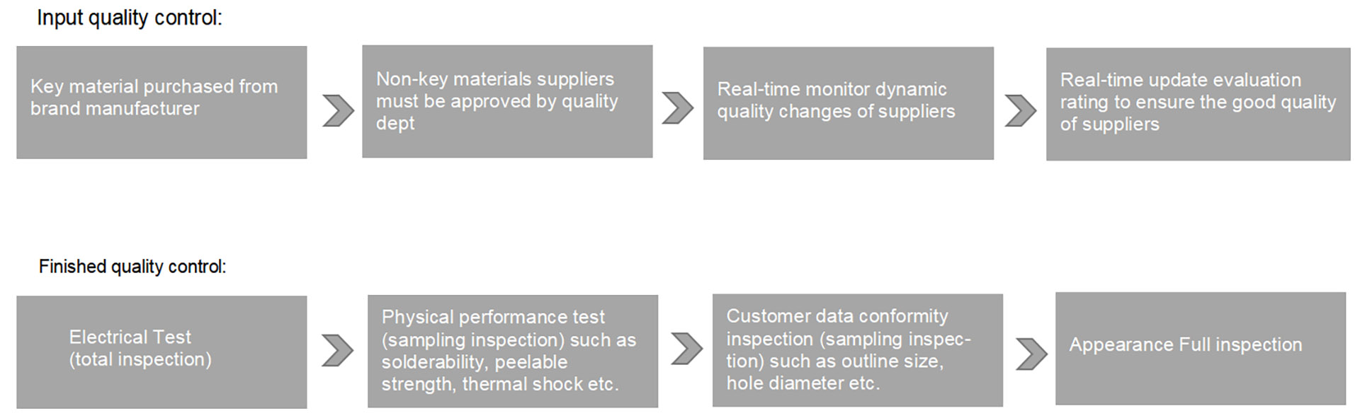
| AOI Testing | Checks for solder pasteChecks for components down to 0201
Checks for missing components, offset, incorrect parts, polarity |
| X-Ray Inspection | X-Ray provides high-resolution inspection of:BGAs/Micro BGAs/Chip scale packages /Bare boards |
| In-Circuit Testing | In-Circuit Testing is commonly used in conjunction with AOI minimizing functional defects caused by component problems. |
| Power-up Test | Advanced Function TestFlash Device Programming
Functional testing |
- IOC incoming inspection
- SPI solder paste inspection
- Online AOI inspection
- SMT first article inspection
- External assessment
- X-RAY-welding inspection
- BGA device rework
- QA inspection
- Anti-static warehousing and shipment
Certificate


FAQ
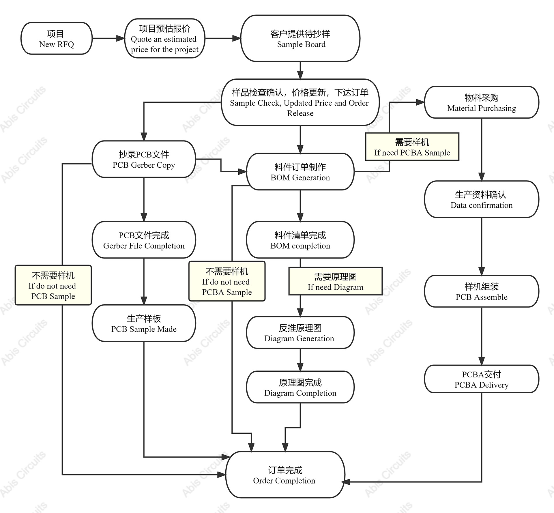
No, we can't accpet picture files, if you no not have gerber file, can you send us sample to copy it.
PCB&PCBA Copy Process:
ABIS CIRCUITS Company is not only trying to give customers a good product, but also pay attention to offering a complete and safe package. Also, we prepare some personalized services for all the orders.
-Common packaging:
- PCB: Sealed bag, Anti-static bags, Suitable carton.
- PCBA: Antistatic foam bags, Anti-static bags, Suitable carton.
- Customized Packaging: The carton outside will be printed the name of the customer address, mark, the customer needs to specify the destination and other information.
-Delivery Tips:
- For small package, we advise to choose byExpress or DDU service is the quickest way.
- For heavy package, the best solution is by sea transportation.
A PCB is a board with copper tracks and pads that connect electronic components. PCBA refers to the assembly of components onto a PCB to create a functioning electronic device.
Solder paste is used to temporarily hold electronic components in place before they are permanently attached to the PCB during the reflow soldering process.
PCBs are tested using various methods, including visual inspection, functional testing, and automated testing equipment.
Our Quality Assuring Procedures as below:
a),Visual Inspection
b),Flying probe, fixture tool
c), Impedance control
d), Solder-ability detection
e), Digital metallograghic microscope
f),AOI (Automated Optical Inspection)
To ensure an accurate quote, be sure to include the following information for your project:
- Complete GERBER files including the BOM list
- Quantities
- Turn time
- Panelization Requirements
- Materials Requirements
- Finish requirements
Bill of materials (BOM) detailing:
a), Manufacturers parts numbers,
b), Components suppliers' parts number (e.g. Digi-key, Mouser, RS )
c), PCBA sample photos if possible.
d), Quantity
ABlS performs 100% visual and AOl inspection as well as performing electrical testing, high voltage testing, impedancecontrol testing, micro-sectioning, thermal shock testing, solder testing, reliability testing, insulating resistance testing, ionic cleanliness testing and PCBA Functional testing.
·With ABIS, customers significantly and effectively reduce their global procurement costs. Behind each service provided by ABIS, is hidden a cost-saving for customers.
. We have two shops together, one is for prototype, quick turn, and small volume making. The other is for mass production also for the HDI board, with highly skilled professional employees, for high-quality products with competitive prices and on-time delivery.
. We provide very professional sales, technical and logistic support, on a worldwide basis with 24 hours of complaint feedback.