Rogers RO4350B high frequency pcb circuit board with 2OZ copper


Basic Info
| Model No.: | PCB-A39 |
| Transport package | Vacuum Packing |
| Certification | UL, ISO9001&14001, SGS, RoHS, Ts16949 |
| Definitions | IPC Class2 |
| Minimum Space/Line | 0.075mm/3mil |
| HS Code | 85340090 |
| Origin: | Made in China |
| Production Capacity: | 720,000 M2/Year |
Product Description
Technical & Capability
| ITEM | CAPABILITY | ITEM | CAPABILITY |
| Layers | 1-20L | Thicker Copper | 1-6OZ |
| Products Type | HF(High-frequency) &(Radio Frequency)board, Imedance controlled board, HDIboard, BGA & Fine Pitch board | Solder Mask | Nanya & Taiyo; LRI & Matt Red. green,yellow, white, blue, black |
| Base material | FR4(Shengyi China,ITEQ, KB A+,HZ),HITG,FrO6,Rogers,Taconic,Argon,Nalco lsola and so on | Finished Surface | Conventional HASL,Lead-free HASL,FlashGold,ENIG (lmmersion Gold) OSP (Entek),lmmersion TiN, lmmersion Silver,Hard Gold |
| Selective Surface treatment | ENIG(immersion Gold) + OSP ,ENIG(immersion Gold) + Gold Finger, Flash Gold Finger, immersionSlive + Gold Finger, Immersion Tin + Gold Finger | ||
| Technical Specification | Minimum line width/gap: 3.5/4mil (laser dril) Minimum hole size: 0.15 mm(mechanical drill/4 mill laser drill) Minimum Annular Ring: 4mil Max Copper thickness: 6Oz Max Production size: 600x1200mm Board Thickness: D/S: 0.2-70mm,Mulltilayers: 0.40-7.Omm Min Solder Mask Bridge: ≥0.08mm Aspect ratio: 15:1 Plugging vias capability: 0.2-0.8mm |
||
| Tolerance | Plated holes Tolerance : ±0.08mm(min±0.05) Non-plated hole tolerance: ±O.05min(min+O/-005mm or +0.05/Omm) Outline Tolerance: ±0.15min(min±0.10mm) Functional test: lnsulating resistance: 50 ohms (normality) Peel off strength: 14N/mm Thermal Stress test: 265C.20 seconds Solder mask hardness: 6H E-test voltage: 50ov±15/-0V 3os Warp and Twist: 0.7%( semiconductor test board 0.3%) |
||
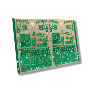
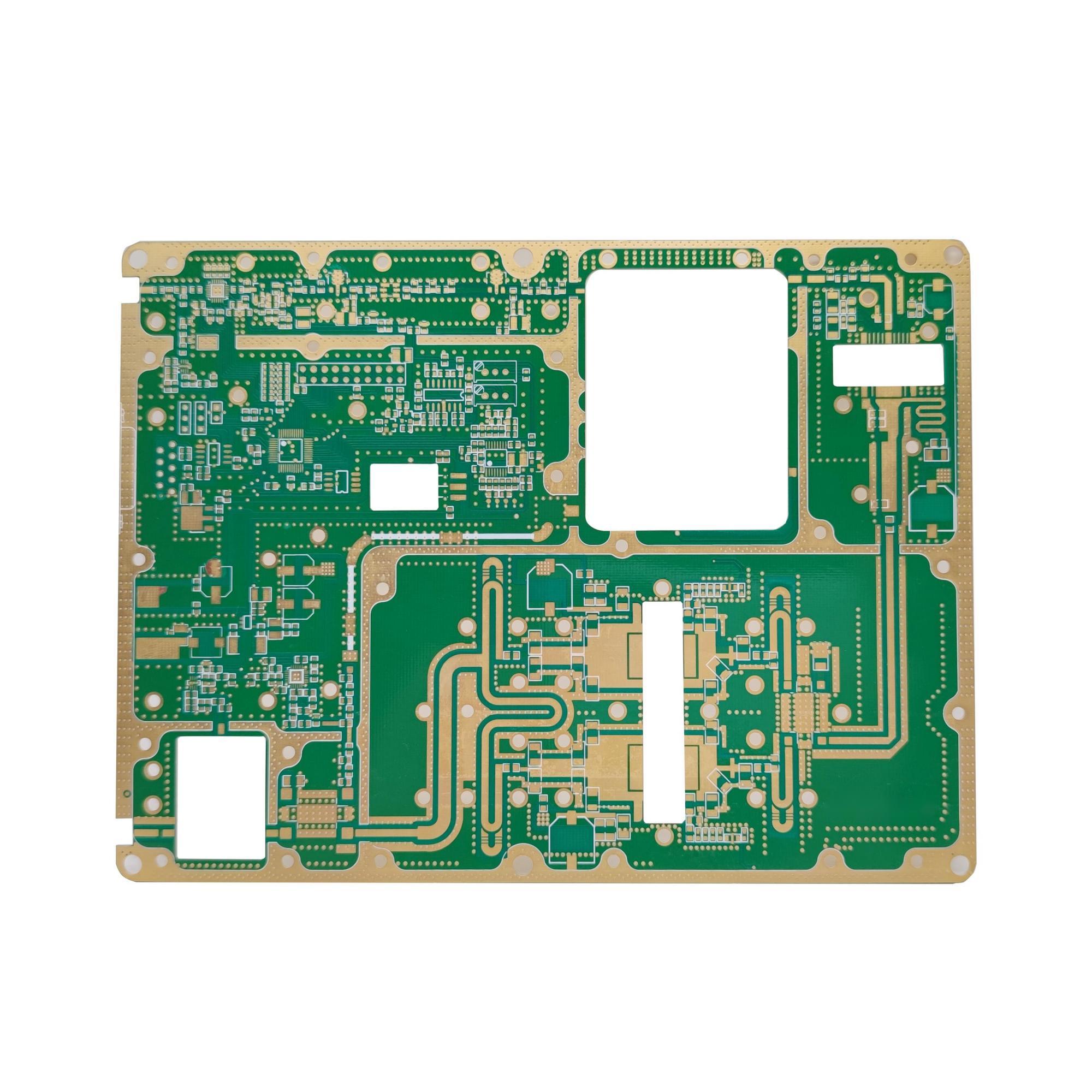
Rogers Board is a type of high-performance printed circuit board (PCB) that is manufactured by Rogers Corporation, a global materials technology company. Rogers Boards are known for their high-frequency and high-speed capabilities, as well as their excellent thermal and electrical stability.
The PCB-A16 is a high-quality Rogers Board that has been designed to meet the rigorous demands of high-speed and high-frequency applications. With a model number of PCB-A16, this circuit board features a two-layer design and measures 165mm by 120mm in dimension.
The PCB-A16 is made from high-quality Rogers base material, a specialized laminate material that offers exceptional thermal and electrical stability. With a board thickness of 2.0mm and a copper thickness of 1.0oz, this circuit board is capable of handling high-speed and high-frequency signals with minimal signal distortion. It also features a surface finish of ENIG 2U’’(min) Filled Vias, which helps to ensure consistent and reliable signal transmission.
This circuit board meets IPC Class2 standards, which ensures that it is manufactured to the highest industry standards for quality and reliability. It has a minimum space/line of 0.075mm/3mil, making it ideal for applications that require high precision and accuracy.
The PCB-A16 comes with a green solder mask color and has no legend color. It is vacuum packed for transportation and comes with certifications such as UL, ISO9001&14001, SGS, RoHS, and Ts16949, ensuring that it meets or exceeds all relevant industry standards. This circuit board is made in China and has a production capacity of 720,000 M2/year.
In summary, the PCB-A16 is an exceptional Rogers 2 Layers High Frequency High Speed Circuit Board that offers exceptional performance, reliability, and signal quality. It is the ideal choice for any application that requires high-speed and high-frequency signal transmission with high precision and accuracy.
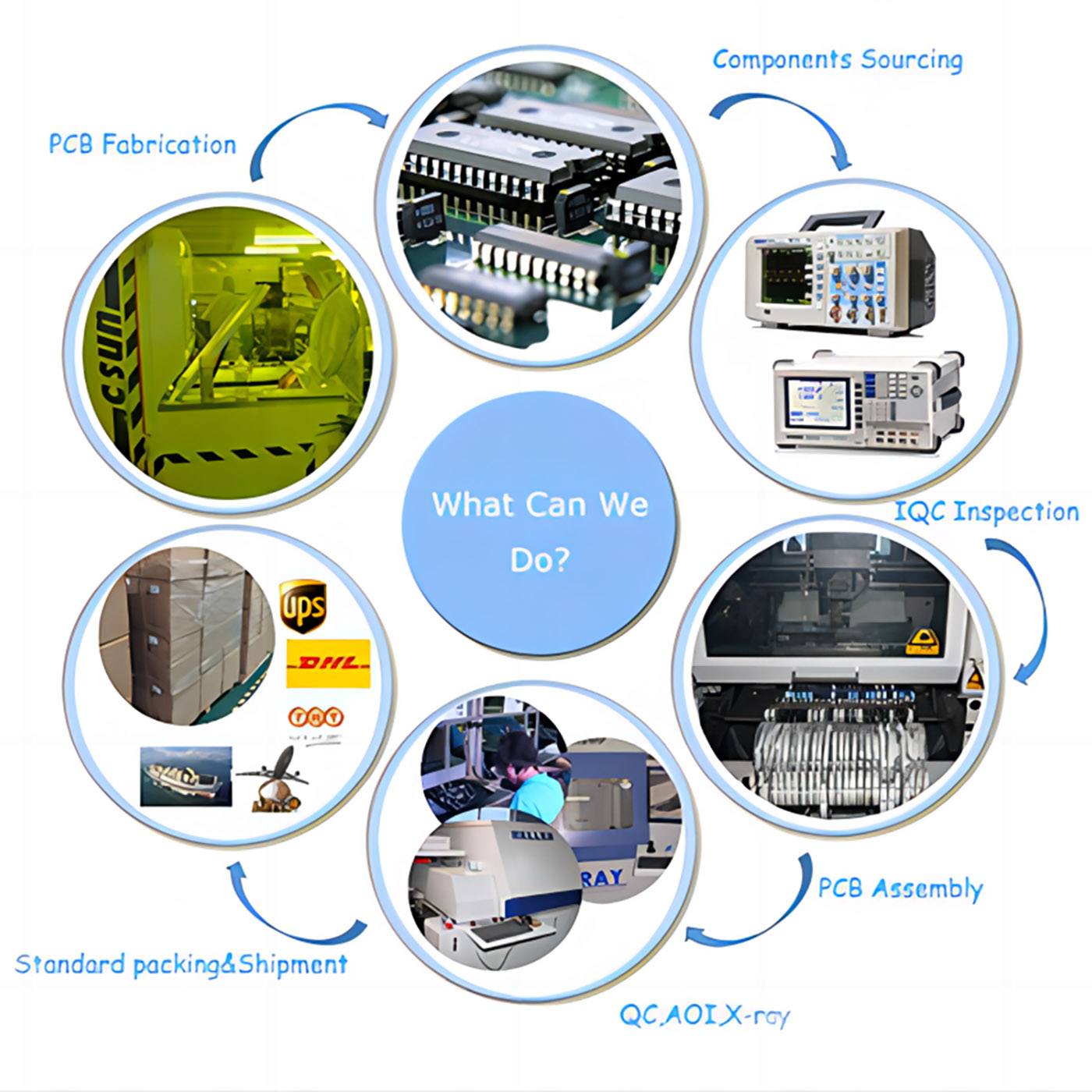
What can ABIS do?
Q/T Lead Time
| Category | Quickest Lead Time | Normal Lead Time |
| Double-sided | 24hrs | 120hrs |
| 4 Layers | 48hrs | 172hrs |
| 6 Layers | 72hrs | 192hrs |
| 8 Layers | 96hrs | 212hrs |
| 10 Layers | 120hrs | 268hrs |
| 12 Layers | 120hrs | 280hrs |
| 14 Layers | 144hrs | 292hrs |
| 16-20 Layers | Depends on the specific requirements | |
| Above 20 Layers | Depends on the specific requirements | |
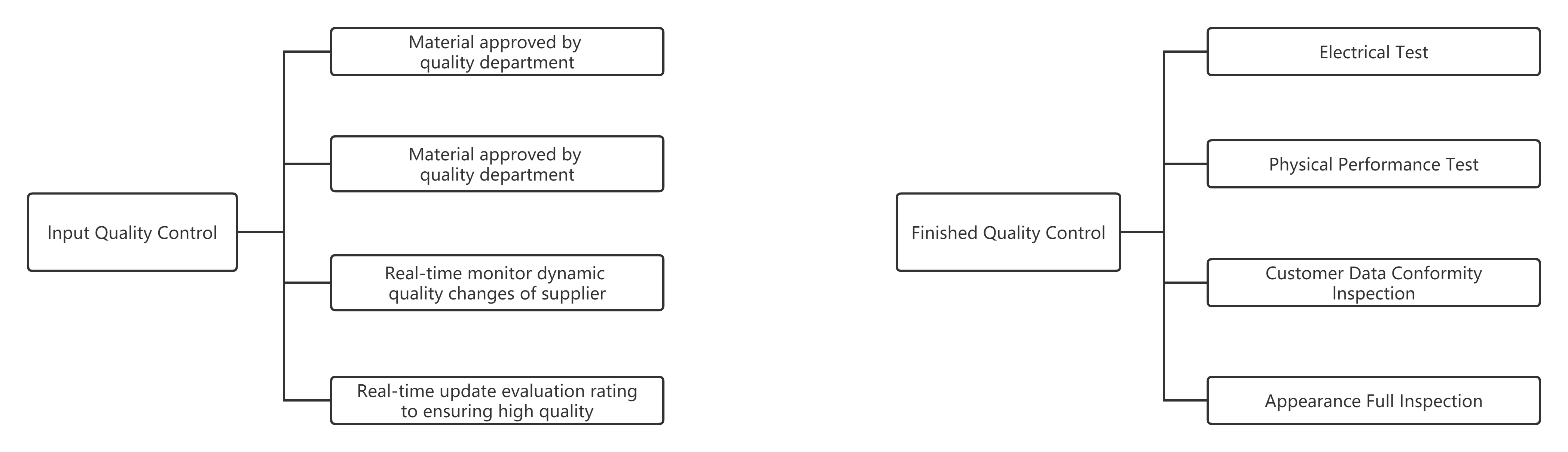
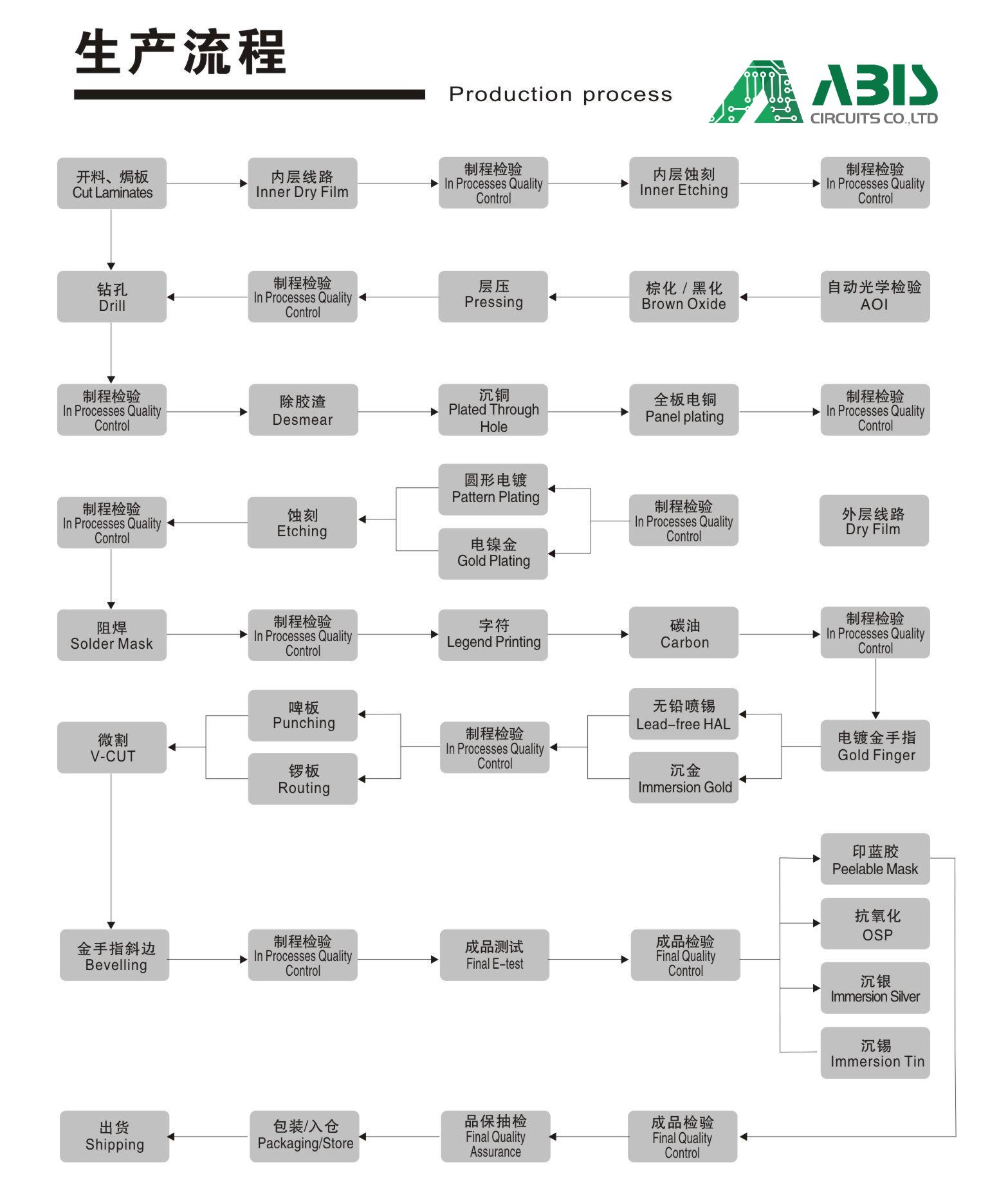
Quality Control
The pass rate of incoming material above 99.9%, the number of mass rejection rates below 0.01%.
ABIS certified facilities control all key processes to eliminate all potential issues before producing.
ABIS utilizes advanced software to perform extensive DFM analysis on incoming data, and uses advanced quality control systems throughout the manufacturing process.
ABIS performs 100% visual and AOI inspection as well as performing electrical testing, high voltage testing, impedance control testing, micro-sectioning, thermal shock testing, solder testing, reliability testing, insulating resistance testing and ionic cleanliness testing.
Certificate


FAQ
Bill of materials (BOM) detailing:
a), Manufacturers parts numbers,
b), Components suppliers' parts number (e.g. Digi-key, Mouser, RS )
c), PCBA sample photos if possible.
d), Quantity
A: It's no problem. If you're a small wholesaler, we would like to grow up with you together.
A: Generally 2-3 days for sample making. The lead time of mass production will depend on the order quantity and the season you place the order.
A: Please send the details inquiry to us, such as the Item Number, Quantity for each item, Quality request, Logo, Payment Terms, Transport method, Discharge place, etc. We will make an accurate quotation for you as soon as possible.
A: Each Customer will have a sale to contact with you. Our working hours: AM 9:00-PM 19:00(Beijing Time) from Monday to Friday. We will reply to your email as soon as quickly during our working time. And you also could contact our sales by cellphone if urgent.
A: Yes, we are pleased to supply module samples to test and check the quality, mixed sample order is available. Please note buyer should pay for the shipping cost.
A: yes, We have a professional drawing engineers' team that you can trust.
A: Yes, we ensure that each piece of PCB, and PCBA will be tested before shipment, and we ensure the goods we sent with good quality.
A: We suggest you use DHL, UPS, FedEx, and TNT forwarder.
ABlS performs 100% visual and AOl inspection as well as performing electrical testing, high voltage testing, impedancecontrol testing, micro-sectioning, thermal shock testing, solder testing, reliability testing, insulating resistance testing, ionic cleanliness testing and PCBA Functional testing.