Custom 8-layer HDI PCB Circuit Board with ENIG surface for Intelligent Electronics


Basic Info
| Model No. | PCB-A55 |
| Dimension | 210*178mm |
| Surface Finished |
ENIG 2U"
|
| Certification | UL, ISO9001&14001, SGS, RoHS, Ts16949 |
| Definitions | IPC Class2 |
| Minimum Space/Line | 0.075mm/3mil |
| Application | Vehicle Tracking |
| Origin | Made in China |
| Production Capacity | 720,000 M2/Year |
Product Description
| ITEM | CAPABILITY | ITEM | CAPABILITY |
| Layers | 1-20L | Thicker Copper | 1-6OZ |
| Products Type | HF(High-frequency) &(Radio Frequency)board, Imedance controlled board, HDIboard, BGA & Fine Pitch board | Solder Mask | Nanya & Taiyo; LRI & Matt Red. green,yellow, white, blue, black |
| Base material | FR4(Shengyi China,ITEQ, KB A+,HZ),HITG,FrO6,Rogers,Taconic,Argon,Nalco lsola and so on | Finished Surface | Conventional HASL,Lead-free HASL,FlashGold,ENIG (lmmersion Gold) OSP (Entek),lmmersion TiN, lmmersion Silver,Hard Gold |
| Selective Surface treatment | ENIG(immersion Gold) + OSP ,ENIG(immersion Gold) + Gold Finger, Flash Gold Finger, immersionSlive + Gold Finger, Immersion Tin + Gold Finger | ||
| Technical Specification | Minimum line width/gap: 3.5/4mil (laser dril) Minimum hole size: 0.15 mm(mechanical drill/4 mill laser drill) Minimum Annular Ring: 4mil Max Copper thickness: 6Oz Max Production size: 600x1200mm Board Thickness: D/S: 0.2-70mm,Mulltilayers: 0.40-7.Omm Min Solder Mask Bridge: ≥0.08mm Aspect ratio: 15:1 Plugging vias capability: 0.2-0.8mm |
||
| Tolerance | Plated holes Tolerance : ±0.08mm(min±0.05) Non-plated hole tolerance: ±O.05min(min+O/-005mm or +0.05/Omm) Outline Tolerance: ±0.15min(min±0.10mm) Functional test: lnsulating resistance: 50 ohms (normality) Peel off strength: 14N/mm Thermal Stress test: 265C.20 seconds Solder mask hardness: 6H E-test voltage: 50ov±15/-0V 3os Warp and Twist: 0.7%( semiconductor test board 0.3%) |
||
Q/T Lead Time
| Category | Quickest Lead Time | Normal Lead Time |
| Double-sided | 24hrs | 120hrs |
| 4 Layers | 48hrs | 172hrs |
| 6 Layers | 72hrs | 192hrs |
| 8 Layers | 96hrs | 212hrs |
| 10 Layers | 120hrs | 268hrs |
| 12 Layers | 120hrs | 280hrs |
| 14 Layers | 144hrs | 292hrs |
| 16-20 Layers | Depends on the specific requirements | |
| Above 20 Layers | Depends on the specific requirements | |
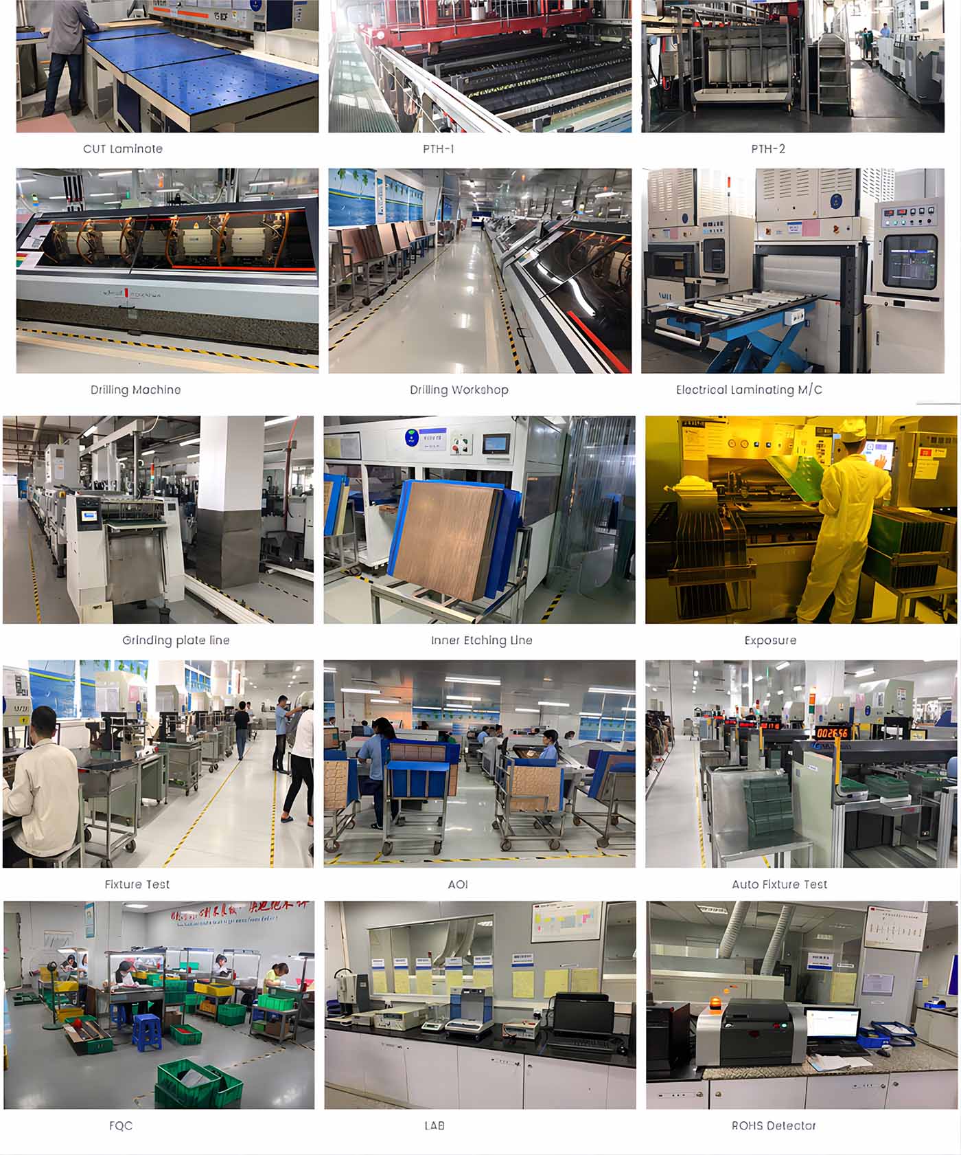
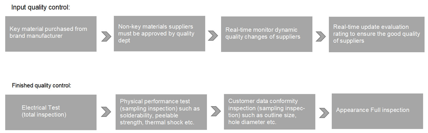
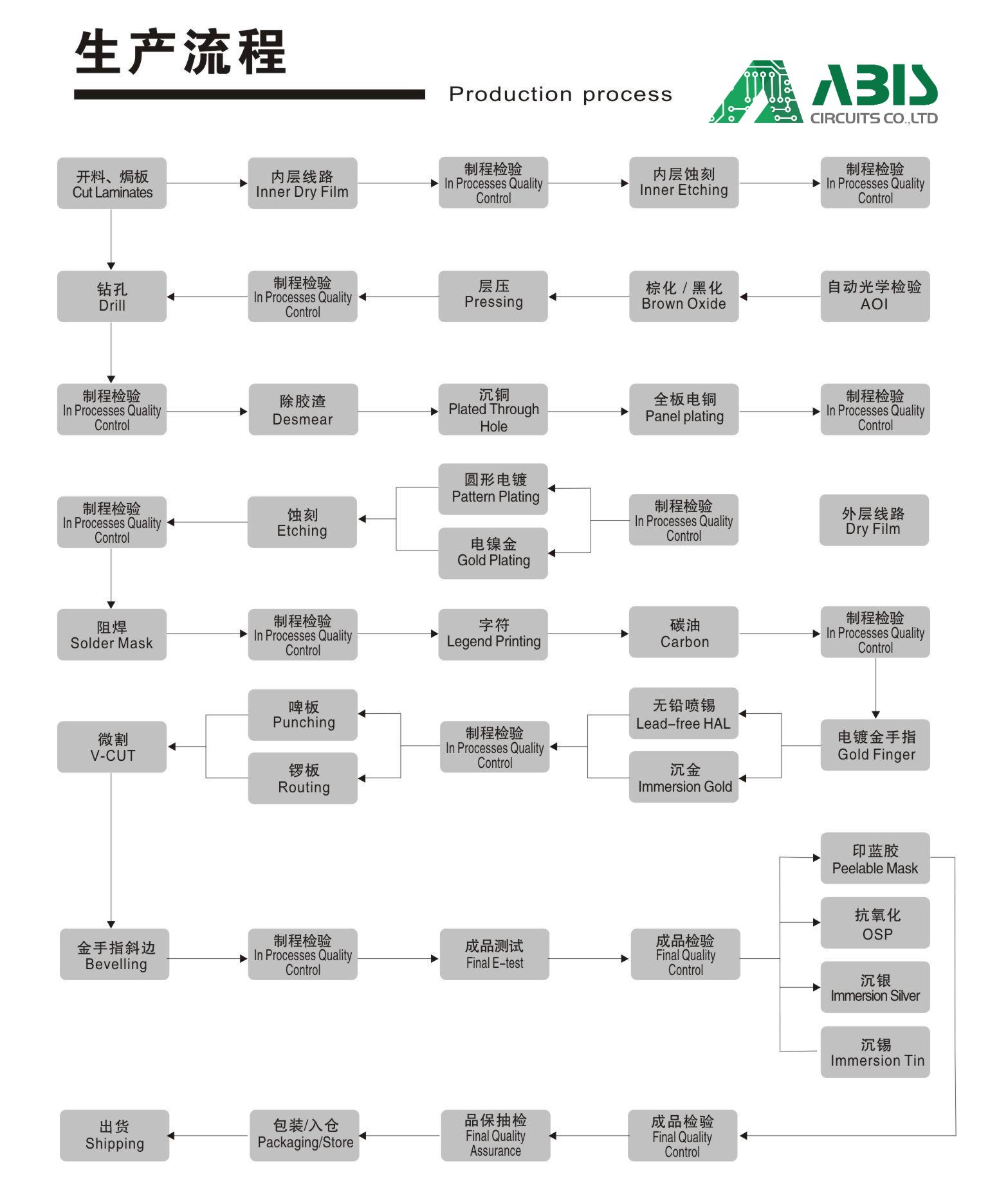
Quality Control
The pass rate of incoming material above 99.9%, the number of mass rejection rates below 0.01%.
ABIS certified facilities control all key processes to eliminate all potential issues before producing.
ABIS utilizes advanced software to perform extensive DFM analysis on incoming data, and uses advanced quality control systems throughout the manufacturing process.
ABIS performs 100% visual and AOI inspection as well as performing electrical testing, high voltage testing, impedance control testing, micro-sectioning, thermal shock testing, solder testing, reliability testing, insulating resistance testing and ionic cleanliness testing.
Certificate


Pre-Sale and After-Sale Service

1 Hour quotation
2 hours of complaint feedback
7*24 hour technical support
7*24 order service
7*24 hour delivery
7*24 production run
Business Terms
-Accepted Delivery Terms
FOB, CIF, EXW, FCA, CPT, DDP, DDU, Express Delivery, DAF
-Accepted Payment Currency
USD, EUR, CNY.
-Accepted Payment Type
T/T, PayPal, Western Union.
Packaging & Delivery
ABIS CIRCUITS Company is not only trying to give customers a good product, but also pay attention to offering a complete and safe package. Also, we prepare some personalized services for all the orders.
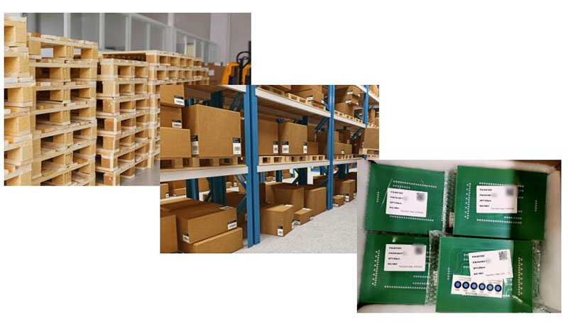
Common packaging:
PCB: Sealed bag, Anti-static bags, Suitable carton.
PCBA: Antistatic foam bags, Anti-static bags, Suitable carton.
Customized Packaging: The carton outside will be printed the name of the customer address, mark, the customer needs to specify the destination and other information.
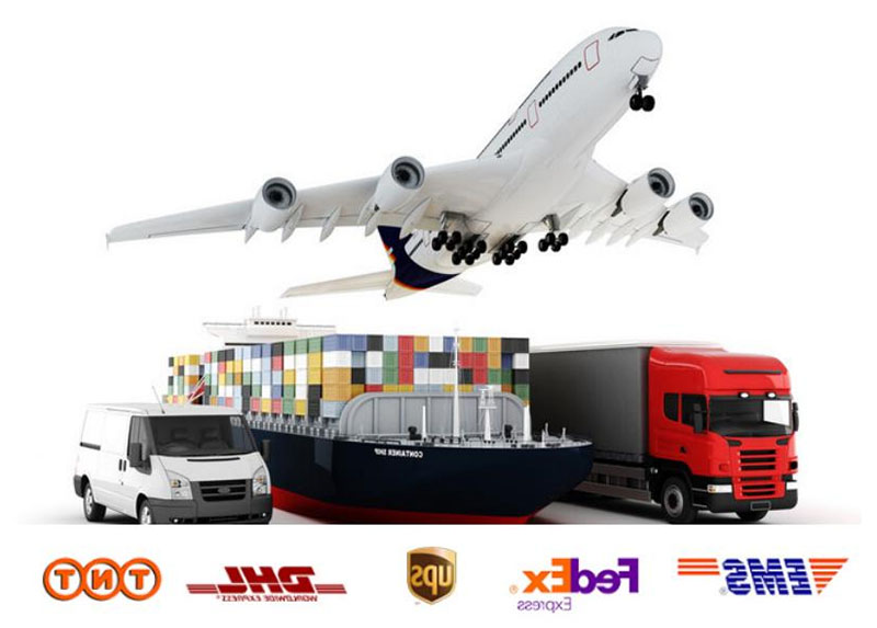
Delivery Tips:
For small package, we advise to choose by Express or DDU service is the quickest way.
For heavy package, the best solution is by sea transportation.
FAQ
A: Main Suppliers(FR4): Kingboard (Hong Kong), NanYa (Taiwan), and Shengyi (China), If others, please RFQ.
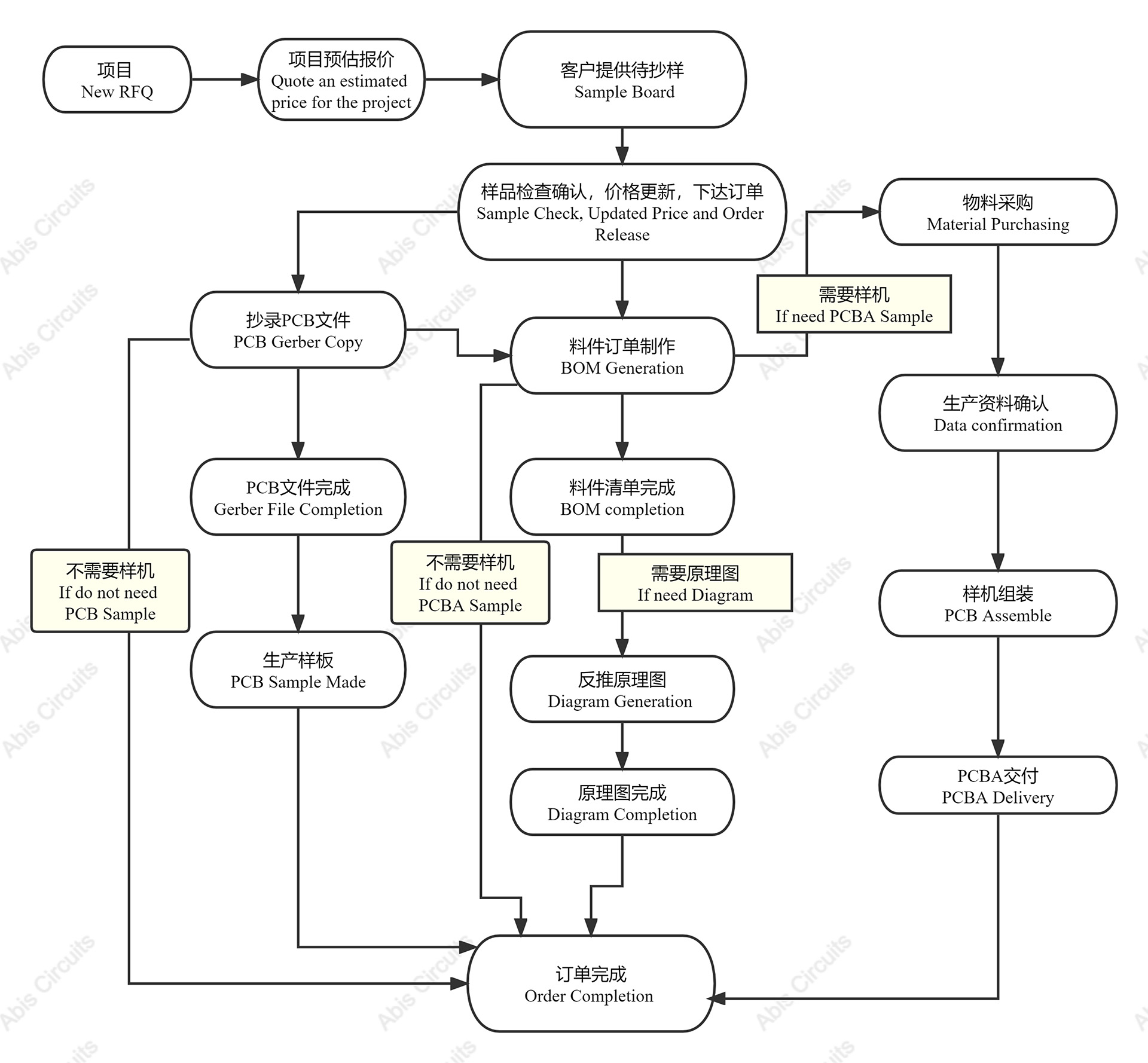
A: Generally 2-3 days for sample making. The lead time of mass production will depend on the order quantity and the season you place the order.
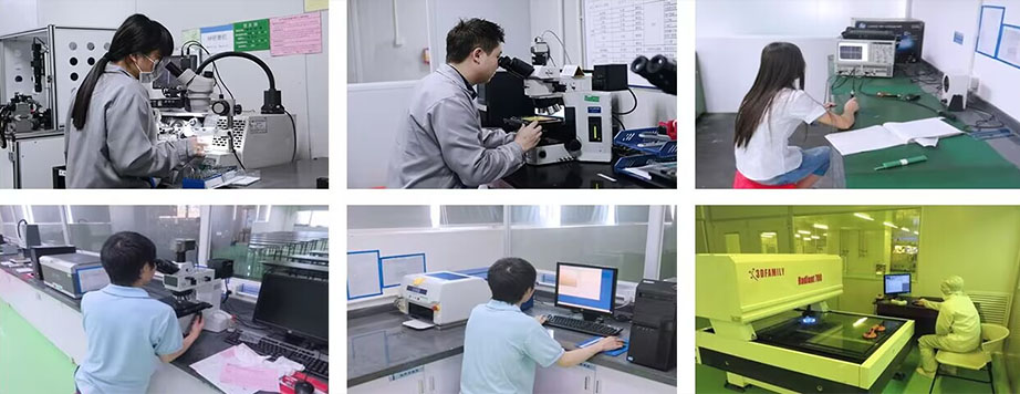
Our Quality Assuring Procedures as below:
a),Visual Inspection
b),Flying probe, fixture tool
c), Impedance control
d), Solder-ability detection
e), Digital metallograghic microscope
f),AOI (Automated Optical Inspection)
A:
| Production capacity of hot-sale products | |
| Double Side/Multilayer PCB Workshop | Aluminum PCB Workshop |
| Technical Capability | Technical Capability |
| Raw materials: CEM-1, CEM-3, FR-4(High TG), Rogers, TELFON | Raw materials: Aluminum base, Copper base |
| Layer: 1 layer to 20 Layers | Layer: 1 layer and 2 Layers |
| Min.line width/space: 3mil/3mil(0.075mm/0.075mm) | Min.line width/space: 4mil/4mil(0.1mm/0.1mm) |
| Min.Hole size: 0.1mm(dirilling hole) | Min. Hole size: 12mil(0.3mm) |
| Max. Board size: 1200mm* 600mm | Max.Board size: 1200mm* 560mm(47in* 22in) |
| Finished board thickness: 0.2mm- 6.0mm | Finished board thickness: 0.3~ 5mm |
| Copper foil thickness: 18um~280um(0.5oz~8oz) | Copper foil thickness: 35um~210um(1oz~6oz) |
| NPTH Hole Tolerance: +/-0.075mm, PTH hole Tolerance: +/-0.05mm | Hole position tolerance: +/-0.05mm |
| Outline Tolerance: +/-0.13mm | Routing outline tolerance: +/ 0.15mm; punching outline tolerance:+/ 0.1mm |
| Surface finished: Lead-free HASL, immersion gold(ENIG), immersion silver, OSP, gold plating, gold finger, Carbon INK. | Surface finished: Lead free HASL, immersion gold(ENIG), immersion silver, OSP etc |
| Impedance control tolerance: +/-10% | Remain thickness tolerance: +/-0.1mm |
| Production capability: 50,000 s.q.m/month | MC PCB Production capability: 10,000 s.q.m/month |
A: ABlS performs 100% visual and AOl inspection as well as performing electrical testing, high voltage testing, impedancecontrol testing, micro-sectioning, thermal shock testing, solder testing, reliability testing, insulating resistance testing, ionic cleanliness testing and PCBA Functional testing.
A: yes, We have a professional drawing engineers' team that you can trust.
A: Yes, we ensure that each piece of PCB, and PCBA will be tested before shipment, and we ensure the goods we sent with good quality.
On time delivery rate is more than 95%
a),24 hours fast turn for double side prototype PCB
b),48hours for 4-8 layers prototype PCB
c),1 hour for quotation
d),2 hours for engineer question/Complaint feedback
e),7-24 hours for technical support/order service/manufacturing operations
Why choose us?
·With ABIS, customers significantly and effectively reduce their global procurement costs. Behind each service provided by ABIS, is hidden a cost-saving for customers.
. We have two shops together, one is for prototype, quick turn, and small volume making. The other is for mass production also for HDI board, with highly skilled professional employees, for high-quality products with competitive price and on-time delivery.
. We provide very professional sales, technical and logistic support, on a worldwide basis. hours complaint feedback.
Please keep us informed of any interest!
ABIS cares about every your order even 1 piece!