
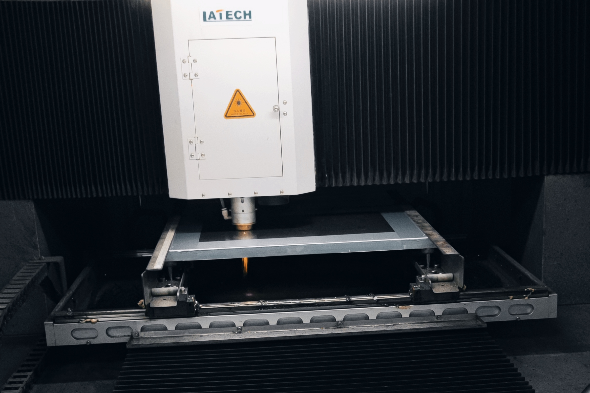
In the process of PCB manufacturing, the production of a Steel Stencil (also known as a "stencil") is carried out to accurately apply solder paste onto the solder paste layer of the PCB. The solder paste layer, also referred to as the "paste mask layer," is a part of the PCB design file used to define the positions and shapes of solder paste. This layer is visible before the surface mount technology (SMT) components are soldered onto the PCB, indicating where the solder paste needs to be placed. During the soldering process, the steel stencil covers the solder paste layer, and solder paste is precisely applied onto the PCB pads through the holes on the stencil, ensuring accurate soldering during the subsequent component assembly process.
Therefore, the solder paste layer is an essential element in producing the steel stencil. In the early stages of PCB manufacturing, the information about the solder paste layer is sent to the PCB manufacturer, who generates the corresponding steel stencil to ensure the accuracy and reliability of the soldering process.
In PCB (Printed Circuit Board) design, the "pastemask" (also known as "solder paste mask" or simply "solder mask") is a crucial layer. It plays a vital role in the soldering process for assembling surface mount devices (SMDs).
The function of the steel stencil is to prevent solder paste from being applied to areas where soldering should not occur when soldering SMD components. Solder paste is the material used to connect SMD components to the PCB pads, and the pastemask layer acts as a "barrier" to ensure that solder paste is applied only to specific soldering areas.
The design of the pastemask layer is highly significant in the PCB manufacturing process as it directly influences the soldering quality and overall performance of SMD components. During PCB design, designers need to carefully consider the layout of the pastemask layer, ensuring its alignment with other layers, such as the pad layer and component layer, to guarantee the accuracy and reliability of the soldering process.
Design Specifications for the Solder Mask Layer (Steel Stencil) in PCB:
In PCB design and manufacturing, the process specifications for the Solder Mask Layer (also known as the Steel Stencil) are typically defined by industry standards and manufacturer requirements. Here are some common design specifications for the Solder Mask Layer:
1. IPC-SM-840C: This is the standard for the Solder Mask Layer established by IPC (Association Connecting Electronics Industries). The standard outlines the performance, physical characteristics, durability, thickness, and solderability requirements for the solder mask.
2. Color and Type: The solder mask can come in different types, such as Hot Air Solder Leveling (HASL) or Electroless Nickel Immersion Gold (ENIG), and different types may have distinct specification requirements.
3. Coverage of Solder Mask Layer: The solder mask layer should cover all the areas that require soldering of components, while ensuring proper shielding of areas that should not be soldered. The solder mask layer should also avoid covering component mounting locations or silk-screen markings.
4. Clarity of Solder Mask Layer: The solder mask layer should have good clarity to ensure clear visibility of the edges of solder pads and to prevent solder paste from overflowing into undesired areas.
5. Thickness of Solder Mask Layer: The thickness of the solder mask layer should comply with standard requirements, usually within a range of several tens of micrometers.
6. Pin Avoidance: Some special components or pins may need to remain exposed in the solder mask layer to meet specific soldering requirements. In such cases, the solder mask specifications may require avoiding the application of solder mask in those specific areas.
Complying with these specifications is essential to ensure the quality and accuracy of the solder mask layer, thus improving the success rate and reliability of PCB manufacturing. Additionally, adherence to these specifications helps optimize the performance of the PCB and ensures correct assembly and soldering of SMD components. Collaborating with the manufacturer and following the relevant standards during the design process is a crucial step in ensuring the quality of the steel stencil layer.
Post time: Aug-04-2023


