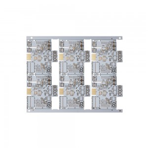
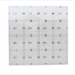
Single-sided Aluminum Base Circuit Board LED strip PCB for Lighting Conversion


Manufacturing info
| Model No. | PCB-A11 |
| Transport package | Vacuum Packing |
| Certification | UL,ISO9001&ISO14001,RoHS |
| Definitions | IPC Class2 |
| Minimum Space/Line | 0.075mm/3mil |
| HS Code | 8534009000 |
| Origin | Made in China |
| Production Capacity | 720,000 M2/Year |
Product Description
ABIS has been manufacturing aluminum PCBs for over 10 years. Our full feature aluminum circuit boards making capabilities and Free DFM Check allows you to get high-quality aluminum PCBs done within budget.
Aluminum PCBs Introduction
Definition
Aluminum base is a CCL, a type of base material of PCBs. It is a composite material composed of copper foil, a dielectric layer, an aluminum base layer and aluminum base membrane with a good heat dissipation. Using a very thin layer of thermally conductive but electrically insulating dielectric, which is laminated between the metal base and the copper layer. The metal base is designed to draw heat away from the circuit through the thin dielectric.
Why is Aluminum used in LED light?
The intense light produced by LEDs creates high levels of heat, which aluminum directs away from components. An aluminum PCB extends the lifespan of an LED device and provides more stability.
Aluminum can actually transfer heat away from vital components, thus minimizing the harmful effect it could have on the circuit board.
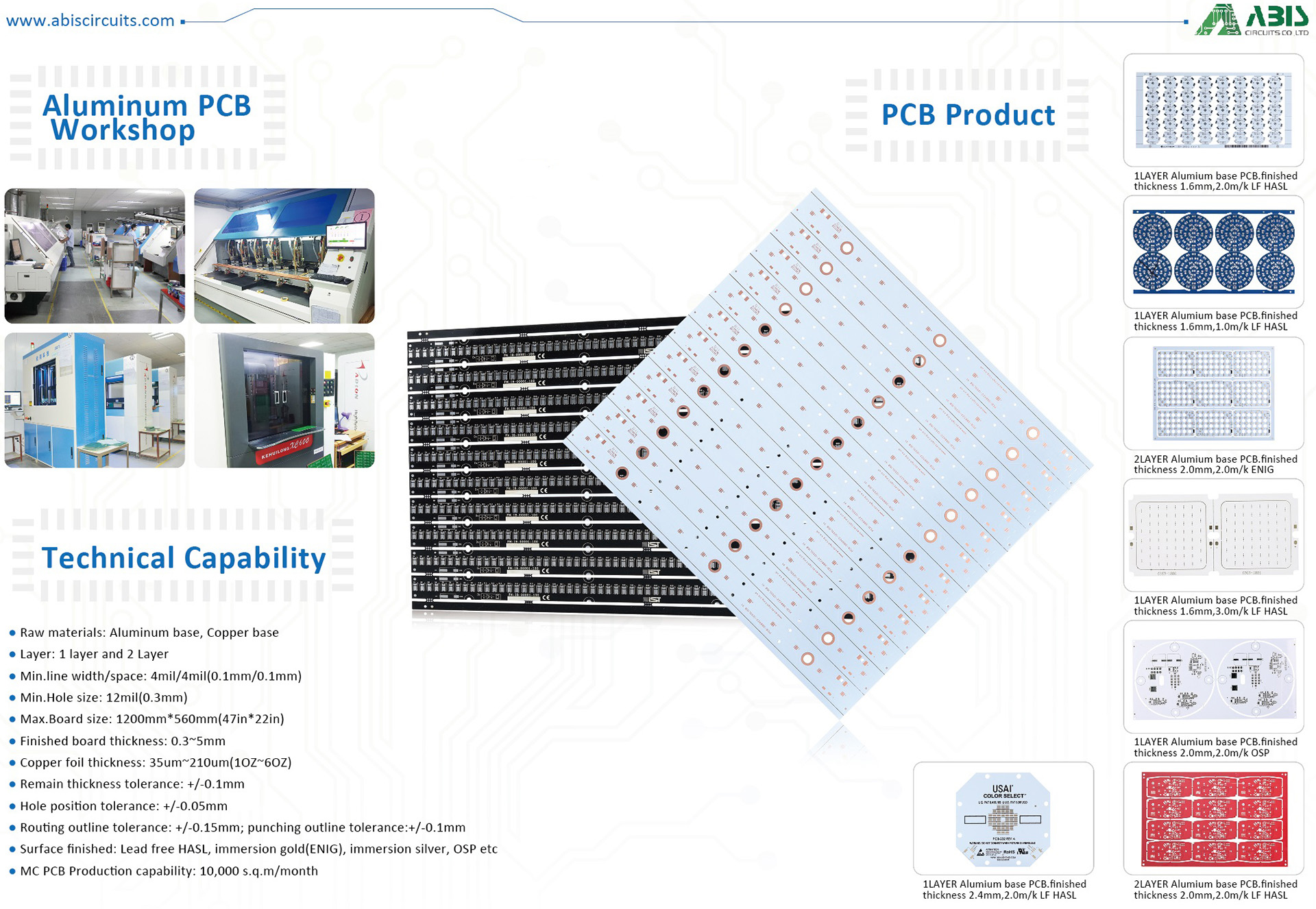
Technical & Capability
|
Item |
Speci. |
|
Layers |
1~2 |
|
Common Finish Board Thickness |
0.3-5mm |
|
Material |
Aluminum Base, Copper base |
|
Max Panel Size |
1200mm*560mm(47in*22in) |
|
Min Hole Size |
12mil(0.3mm) |
|
Min Line Width/Space |
3mil(0.075mm) |
|
Copper Foil Thickness |
35μm-210μm(1oz-6oz) |
|
Common Copper Thickness |
18μm, 35μm, 70μm, 105μm. |
|
Remain Thickness Tolerance |
+/-0.1mm |
|
Routing Outline Tolerance |
+/-0.15mm |
|
Punching Outline Tolerance |
+/-0.1mm |
|
Solder Mask Type |
LPI(liquid photo image) |
|
Mini. Solder Mask Clearance |
0.05mm |
|
Plug Hole Diameter |
0.25mm--0.60mm |
|
Impedance Control Tolerance |
+/-10% |
|
Surface finish |
Lead free HASL, immersion gold(ENIG), immersion sliver, OSP, etc |
|
Solder Mask |
Custom |
|
Silkscreen |
Custom |
|
MC PCB Production Capacity |
10,000 s.q.m/monthly |
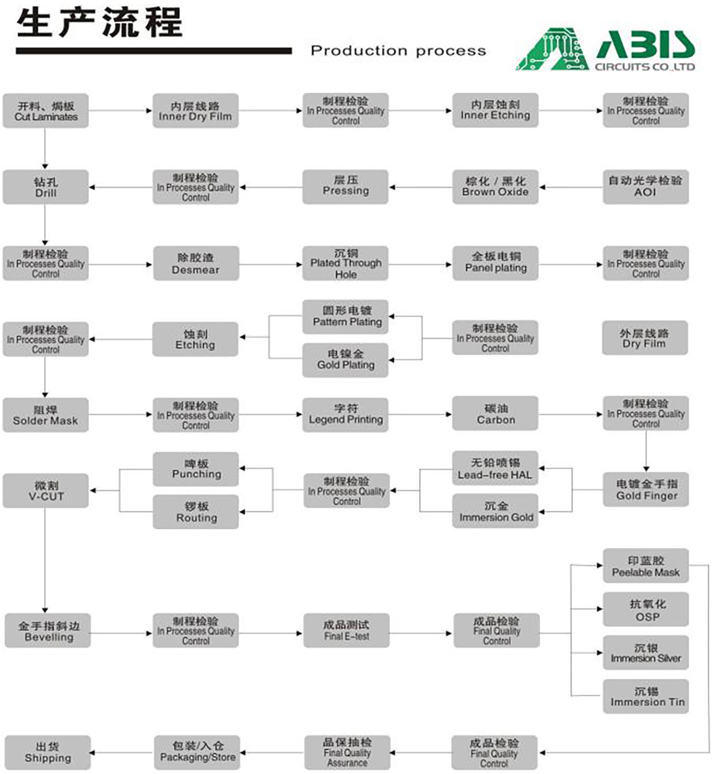
PCB Production Process
Q/T Lead Time
As the current mainstream, we mostly do single aluminum PCB, while it is more difficult to do double sided aluminum PCB.
|
Small Batch Volume ≤1 sq meter |
Working Days |
Mass Production >1 sq meter |
Working Days |
|
Single Sided |
3-4 Days |
Single Sided |
2-4 weeks |
|
Double Sided |
6-7 Days |
Double Sided |
2.5-5 weeks |
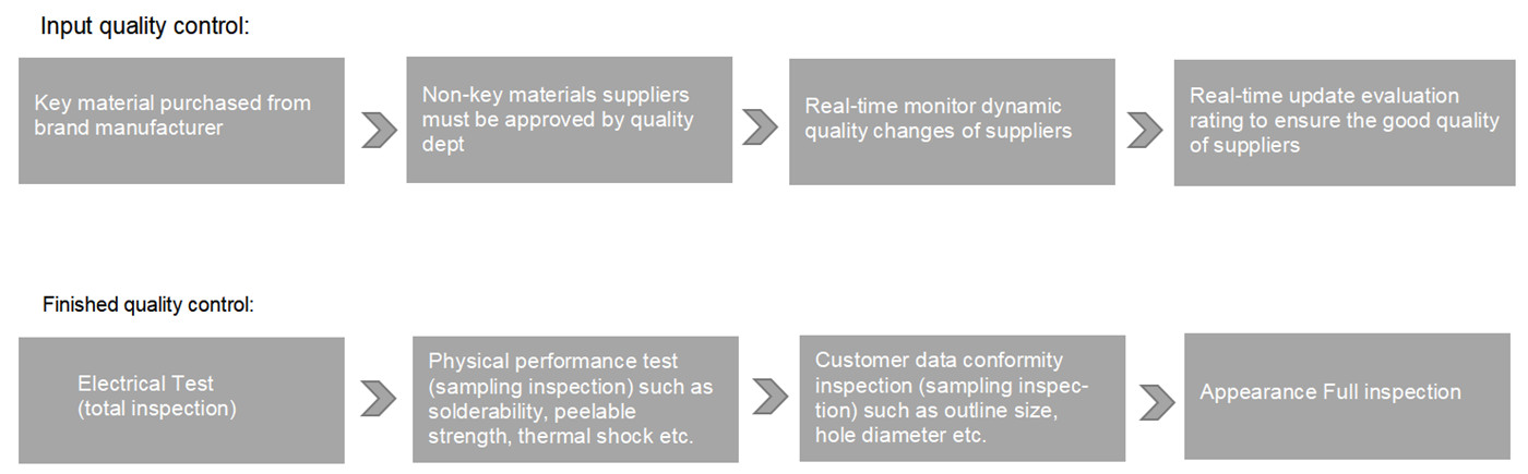
Quality Control
The pass rate of incoming material above 99.9%, the number of mass rejection rates below 0.01%.
ABIS certified facilities control all key processes to eliminate all potential issues before producing.
ABIS utilizes advanced software to perform extensive DFM analysis on incoming data, and uses advanced quality
control systems throughout the manufacturing process.
ABIS performs 100% visual and AOI inspection as well as performing electrical testing, high voltage testing, impedance
control testing, micro-sectioning, thermal shock testing, solder testing, reliability testing, insulating resistance testing and ionic cleanliness testing.
How ABIS Working Out Manufacturing Difficulties of Aluminum PCB?
Raw materials are strictly controlled: The pass rate of incoming material above 99.9%. The number of mass rejection rates is below 0.01%.
Copper Etching Controlled: the copper foil used in Aluminum PCBs is comparatively thicker. If the copper foil is over 3oz however, the etching requires width compensation. With the high precision equipment imported from Germany, the min width/space we can control reaches 0.01mm. The trace width compensation will be designed accurately to avoid the trace width out of tolerance after etching.
High Quality Solder Mask Printing: As we all know, there is a difficulty in solder mask printing of aluminum PCB due to copper thick. This is because if the trace copper is too thick, then the image etched will have a large difference between trace surface and base board and solder mask printing will be difficult. We insist on the highest standards of solder mask oil in the whole process, from the one to the two-time solder mask printing.
Mechanical Manufacturing: To avoid reducing electrical strength caused by the mechanical manufacturing process, involves mechanical drilling, molding and v-scoring etc. Therefore, for low-volume manufacturing of products, we prioritize using the electric milling and professional milling cutter. Also, we pay high attention to adjusting the drilling parameters and preventing burr from generating.
Certificate


Specification of Aluminum Based Copper-clad Laminate
|
Item |
Test a |
AL-01-P Specification |
AL-01-A Specification |
AL-01-L Specification |
Unit |
|
| Thermal Conductivity |
A |
0.8±20% |
1.3±20% |
2.0±20% |
3.0±20% |
W/m.K |
| Thermal Resistance | 0.85 | 0.65 | 0.45 | 0.3 | ℃W | |
| Solder Resistance | 288deg.c | 120 | 120 | 120 | 120 | Sec |
| Peel Strength Normal Status |
A Thermal |
1.2 |
1.2 |
1.2 |
1.2 |
N/mm |
| Volume resistivity Normal Status |
C-96/35/90 E- |
108 |
108 |
108 |
108 |
MΩ.CM |
| Surface Resistivity Normal Status |
C-96/35/90 E- |
107 |
107 |
107 |
107 |
MΩ |
| Dielectric Constant | C-96/35/90 | 4.2 | 4.9 | 4.9 | 4.9 | 1MH2 |
| Dissipation Factor | C-96/35/90 | ≤0.02 | ≤0.02 | ≤0.02 | ≤0.02 | 1MH2 |
| Water Absorption | 0.1 | 0.1 | 0.1 | 0.1 | % | |
| Breakdown Volte | D-48/50+D-0.5/23 | 3 | 3 | 3 | 3 | KV/DC |
| Insulation Strength | A | 30 | 30 | 30 | 30 | KV/mm |
| Raise Camber | A | 0.5 | 0.5 | 0.5 | 0.5 | % |
| Flameability | UL94 | V-0 | V-0 | V-0 | V-0 | |
| CTi | IEC60112 | 600 | 600 | 600 | 600 | V |
| TG | 150 | 130 | 130 | 130 | ℃ | |
|
Product Thickness |
The actinium screen is thick : 1 oz~15 oz, The aluminium board is thick: |
|
Product Specification |
1000×1200 500×1200(mm) |
| • Voice frequency equipment input,output amplifer,compensating capacitor, the voice frequency amplifier,preamplifier, power amplifier etc.
• Power supply equipment: series voltage regulation, switch modulator,and DC-AC transducer …etc. • Telecommunication electron equipment high frequency amplifier, fiter telephone, send a telegram telephone. • Office automation:the printer driver,big electronic display substrate and thermal print A class. • Autocar the igniter, power supply modulator and swap transform machine, power supply controller, become only system etc. • Calculator. CPU board, soft pan driver,and power supply device …etc. • Power mold mass:change to flow a machine, solid relay, commuter bridge etc. • LED light, heat and water expense:big power LED light, LED wall etc |
|
FAQ
a),1 Hour quotation
b),2 hours of complaint feedback
c),7*24 hour technical support
d),7*24 order service
e),7*24 hour delivery
f),7*24 production run
Generally 2-3 days for sample making. The lead time of mass production will depend on the order quantity and the season you place the order.
Checked within 12 hours. Once Engineer's question and working file checked, we'll start the production.
ISO9001, ISO14001,UL USA& USA Canada,IFA16949, SGS, RoHS report.
|
Production capacity of hot-sale products |
|
|
Double Side/Multilayer PCB Workshop |
Aluminum PCB Workshop |
|
Technical Capability |
Technical Capability |
|
Raw materials: CEM-1, CEM-3, FR-4(High TG), Rogers, TELFON |
Raw materials: Aluminum base, Copper base |
|
Layer: 1 layer to 20 Layers |
Layer: 1 layer and 2 Layers |
|
Min.line width/space: 3mil/3mil(0.075mm/0.075mm) |
Min.line width/space: 4mil/4mil(0.1mm/0.1mm) |
|
Min.Hole size: 0.1mm(dirilling hole) |
Min. Hole size: 12mil(0.3mm) |
|
Max. Board size: 1200mm* 600mm |
Max.Board size: 1200mm* 560mm(47in* 22in) |
|
Finished board thickness: 0.2mm- 6.0mm |
Finished board thickness: 0.3~ 5mm |
|
Copper foil thickness: 18um~280um(0.5oz~8oz) |
Copper foil thickness: 35um~210um(1oz~6oz) |
|
NPTH Hole Tolerance: +/-0.075mm, PTH hole Tolerance: +/-0.05mm |
Hole position tolerance: +/-0.05mm |
|
Outline Tolerance: +/-0.13mm |
Routing outline tolerance: +/ 0.15mm; punching outline tolerance:+/ 0.1mm |
|
Surface finished: Lead-free HASL, immersion gold(ENIG), immersion silver, OSP, gold plating, gold finger, Carbon INK. |
Surface finished: Lead free HASL, immersion gold(ENIG), immersion silver, OSP etc |
|
Impedance control tolerance: +/-10% |
Remain thickness tolerance: +/-0.1mm |
|
Production capability: 50,000 s.q.m/month |
MC PCB Production capability: 10,000 s.q.m/month |
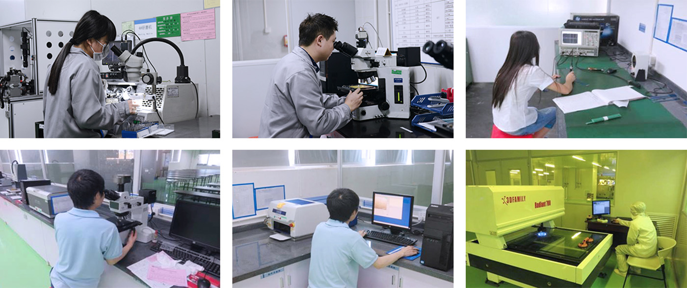
Our Quality Assuring Procedures as below:
a),Visual Inspection
b),Flying probe, fixture tool
c), Impedance control
d), Solder-ability detection
e), Digital metallograghic microscope
f),AOI (Automated Optical Inspection)
Yes, we are pleased to supply module samples to test and check the quality, mixed sample order is available. Please note buyer should pay for the shipping cost.
Our prices are subject to change depending on supply and other market factors. We will send you an updated price list after your company send inquiry to us.
We provide freight according to the rules setting by express company, no more extra charge.
On time delivery rate is more than 95%
a),24 hours fast turn for double side prototype PCB
b),48hours for 4-8 layers prototype PCB
c),1 hour for quotation
d),2 hours for engineer question/Complaint feedback
e),7-24 hours for technical support/order service/manufacturing operations